OLED (organic light-emitting diode) device with all-inorganic auxiliary layer and preparation method thereof

An auxiliary layer and inorganic technology, applied in the field of all-inorganic auxiliary layer OLED devices and their preparation, can solve problems such as cracking, limited industrialization process of organic light-emitting devices, and environmental damage, and achieve improved device stability, rich and delicate colors, The effect of improving productivity

Inactive Publication Date: 2012-08-29
西安宙斯光电科技有限公司
View PDF2 Cites 0 Cited by
  • Summary
  • Abstract
  • Description
  • Claims
  • Application Information

AI Technical Summary

Problems solved by technology

[0005] 1. The price of ITO glass is high, and the mineral reserves of the dopant element indium are low, and the price tends to rise year by year, which limits the industrialization process of organic light-emitting devices
[0006] 2. In order to obtain a relatively uniform surface morphology and a crystal structure with high electrical conductivity when ITO is sputtered into a film, the film must be formed at about 300°C and kept for a period of time for annealing. This process is not suitable for flexible plastics that are not resistant to high temperatures. The substrate is greatly damaged, so the charge injection performance of the ITO electrode on the flexible plastic substrate is quite different from that of the glass substrate ITO, and the price is very expensive, and it has no practical value.
[0007] 3. The entire ITO glass needs to use strong acid to etch the metal oxide of the anode in the process of forming pixels, which is complicated in process and damages the environment
In addition, organic compounds may also generate free radicals under the excitation of the OLED device itself or voltage, causing cracking

Method used


Image

  • OLED (organic light-emitting diode) device with all-inorganic auxiliary layer and preparation method thereof
  • OLED (organic light-emitting diode) device with all-inorganic auxiliary layer and preparation method thereof
  • OLED (organic light-emitting diode) device with all-inorganic auxiliary layer and preparation method thereof

Examples


Embodiment 1

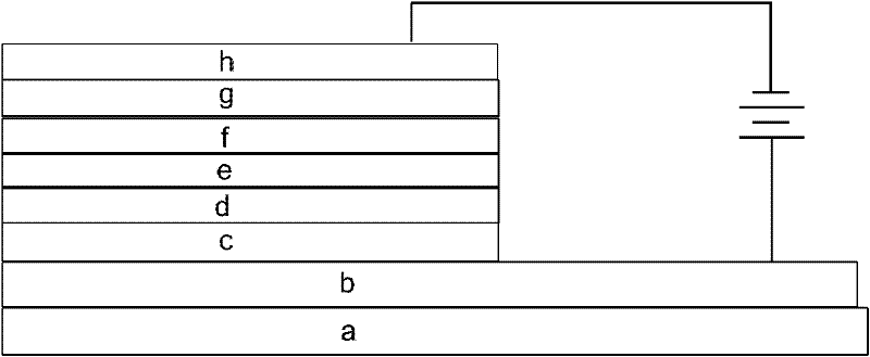
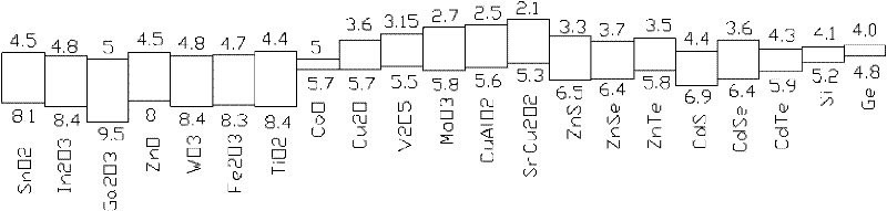
[0050] The flat glass substrate was cleaned with ultrasonic waves in an aqueous solution containing a decontamination agent, rinsed with distilled water and ethanol, and dried. Transfer the substrate to a vacuum thermal evaporation chamber. Sputter aluminum anode 15nm on the glass substrate, respectively sputter on the anode in sequence: molybdenum oxide 15nm; silicon oxide 1nm; molybdenum oxide 25nm; It is 3:1. Then thermally evaporated AlQ 3 75nm; ZnS 8nm; ZnSe 30nm; LiF 1nm; finally thermal sublimation evaporated aluminum 100nm to form the cathode. The deposition rate was kept at 2 angstroms / s for organic materials, 1 angstroms / s for LiF, 5 angstroms / s for aluminum, 2 angstroms / s for silicon oxide, 3 angstroms / s for molybdenum oxide, and finally with Glass cover plate encapsulation, the formed device structure is as follows:

[0051] Glass / Al(15nm) / MoO 3 (15nm) / SiO 2 (1nm) / MoO 3 (25nm) / MoO 3 : SiO 2 3:1 (30nm) / AlQ 3 (75nm) / ZnS(8nm) / ZnSe(30nm) / LiF(1nm) / Al(100nm)....

Embodiment 2

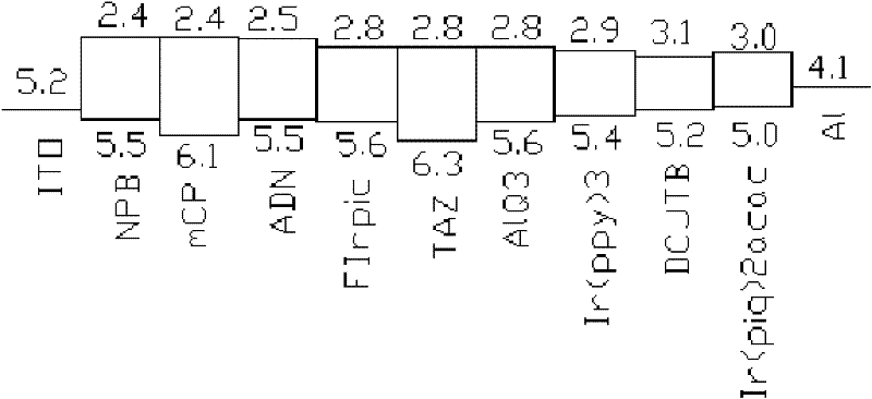
[0064] Sputtering of fluorine-doped tin oxide (SnO 2 : F) The flat glass substrate of the anode is cleaned with ultrasonic waves, then rinsed with distilled water and ethanol and dried. Transfer the substrate to a vacuum thermal evaporation chamber. in SnO 2 : Molybdenum oxide 8nm is sputtered on the F glass substrate, and NPB and molybdenum oxide mixed layer are vapor-deposited 100nm, wherein the molar ratio of NPB and molybdenum oxide is 40:60; AlQ 3 90nm; ZnS 8nm; ZnSe 30nm; LiF 1nm; finally thermal sublimation evaporated aluminum 100nm to form the cathode. The deposition rate was kept at 2 Å / s for organic materials, 1 Å / s for LiF, 5 Å / s for Al, 2 Å / s for ZnS, ZnSe, 3 Å / s for MoO, and finally Encapsulated with a glass cover, the resulting device structure is as follows:

[0065] Glass / SnO 2 :F / MoO 3 (8nm) / NPB:MoO 3 40:60(100nm) / AlQ 3 (90nm) / ZnS(8nm) / ZnSe(30nm) / LiF(1nm) / Al(100nm).

[0066] where SnO 2 : F is a cheap anode, molybdenum oxide is the hole injection l...

Embodiment 3

[0069] The flat glass substrate was cleaned with ultrasonic waves in an aqueous solution containing a decontamination agent, rinsed with distilled water and ethanol, and dried. Transfer the substrate to a vacuum thermal evaporation chamber. Chromium reflective layer 10nm sputtered on glass substrate, aluminum cathode 30nm, LiF 1nm sputtered on cathode; TiO 2 3nm; ZnTe 30nm; then thermal sublimation evaporation TPBi and Ir(ppy) 3 The mixed layer of 80nm, in which TPBi and Ir(ppy) 3 Molar ratio of 100:35; molybdenum oxide 120nm; finally thermal sublimation evaporation aluminum 15nm to form the anode. The deposition rate is maintained at 2 angstroms / sec for organic materials, 5 angstroms / sec for aluminum, and for ZnTe, TiO 2 At 2 angstroms / sec, 3 angstroms / sec for molybdenum oxide, and finally encapsulated with a glass cover plate, the formed device structure is as follows:

[0070] Al(15nm) / MoO 3 (120nm) / TPBi:Ir(ppy) 3 100:35(80nm) / ZnTe(30nm) / TiO 2 (3nm) / LiF(1nm) / Al(30n...


PUM

PropertyMeasurementUnit
luminanceaaaaaaaaaa
luminanceaaaaaaaaaa
full width at half maximumaaaaaaaaaa

Abstract

The invention relates to an OLED (organic light-emitting diode) device with an all-inorganic auxiliary layer, which comprises an inorganic anode, an inorganic cathode, the inorganic auxiliary layer and an organic light-emitting layer, wherein the inorganic anode and the inorganic cathode are made of inorganic material; the inorganic auxiliary layer adopts the inorganic material or inorganic material doped with organic material; and the organic light-emitting layer is made of organic light-emitting material. Compared with the prior art, the OLED device has the following advantages: 1) the inorganic auxiliary layer adopts a large amount of the inorganic material, thereby reducing the cost; 2) the stability of the device is greatly improved, and the service life can achieve the commercial standard; 3) the advantage of abundant is kept by refined colors of an organic light-emitting compound in the device; 4) the proportion of the sputtering process is enlarged, and the production efficiency is improved; and 5) the manufacturing process can be started from the anode or the cathode, and the way can be selected flexibly.

Description

【Technical field】 [0001] The invention relates to the technical field of organic electroluminescence, in particular to an all-inorganic auxiliary layer OLED device and a preparation method thereof. 【Background technique】 [0002] Organic electroluminescent device (OLED) is a self-luminous, high-brightness, full-color display light-emitting element, which has an attractive prospect in the field of flat-panel display, and is the key research and development direction of various OLED manufacturers. OLED light-emitting devices are superior to LED devices in that they have rich luminous colors, and corresponding organic compounds can be found in various bands, while LED light sources have few inorganic semiconductor types available, and non-primary color light can only be mixed by three primary color light sources. , the color performance is not delicate enough. At the same time, LEDs cannot make large-area continuous light-emitting surfaces. see figure 1 As shown, the structu...

Claims


Application Information

Patent Timeline
Patent Type & Authority Patents(China)
IPC IPC(8): H01L51/50H01L51/52H01L51/54H01L51/56
Inventor 闵军辉徐宁宋书清
Owner 西安宙斯光电科技有限公司
Why Eureka
Try Eureka