Surface processing method of Auger electron spectrometer detecting sample

A technology of Auger electronics and sample detection, which is applied in the field of integrated circuit manufacturing, can solve the problems of platinum or silver signal weakening, interference, covering, etc., and achieve the effect of reducing charging effect, improving signal-to-noise ratio, and avoiding cost

Inactive Publication Date: 2012-11-21
SEMICON MFG INT (SHANGHAI) CORP
View PDF0 Cites 0 Cited by
  • Summary
  • Abstract
  • Description
  • Claims
  • Application Information

AI Technical Summary

Problems solved by technology

For example, aluminum foil and other conductive substances are used to wrap the Auger electron spectrometer detection sample. However, because the detection sample to be analyzed is very small, it is difficult to locate during the wrapping process, and it is difficult to ensure that the pad area to be analyzed is exposed. Therefore, this The success rate of the method is very low
[0006] The industry also adopts another method to reduce the charging effect, that is, to coat conductive glue such as silver glue or carbon glue on the surface of the detection sample, but this method also has a disadvantage, that is, these conductive glues are very easy to be polluted during the coating process Pad surface, while masking the true condition of the pad surface to be analyzed
[0007] In addition, the industry is also trying to electroplate conductive substances such as platinum or silver on the surface of the detection sample to reduce the charging effect. However, the process of electroplating platinum or silver is also likely to cause contamination on the surface of the detection sample and cause the surface of the pad to be analyzed to be polluted. The actual element signals are weakened or interfered by a large number of platinum or silver signals, which makes it impossible to obtain accurate pad surface composition analysis results

Method used


Image

  • Surface processing method of Auger electron spectrometer detecting sample
  • Surface processing method of Auger electron spectrometer detecting sample
  • Surface processing method of Auger electron spectrometer detecting sample

Examples


Embodiment Construction

[0027] The invention will now be described in more detail with reference to the accompanying drawings, in which preferred embodiments of the invention are shown, it being understood that those skilled in the art may modify the invention described herein and still achieve the advantageous effects of the invention. Therefore, the following description should be understood as the broad knowledge of those skilled in the art, but not as a limitation of the present invention.

[0028] In the interest of clarity, not all features of an actual implementation are described. In the following description, well-known functions and constructions are not described in detail since they would obscure the invention with unnecessary detail. It should be appreciated that in the development of any actual embodiment, numerous implementation details must be worked out to achieve the developer's specific goals, such as changing from one embodiment to another in accordance with system-related or busi...


PUM


Abstract

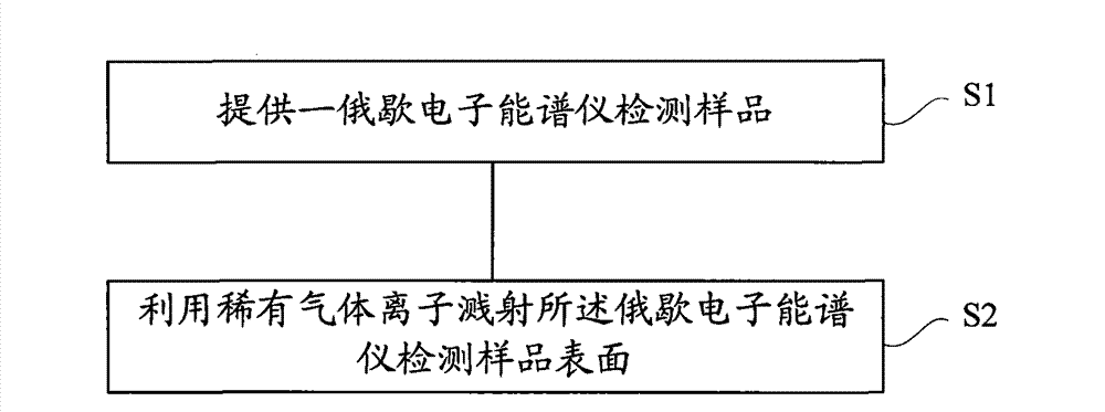
The invention discloses a surface processing method of an Auger electron spectrometer detecting sample, which comprises the following steps of providing the Auger electron spectrometer detecting sample; and utilizing rare gas ions to sputter the surface of the Auger electron spectrometer detecting sample. The method is simple and practical, has low cost, can rapidly and effectively reduce the charge effect and has no damage to the surface of the detecting sample requiring to be proximately analyzed so as to ensure obtaining the accurate proximate analysis result of the surface of the detecting sample and enhance the yield of the product.

Description

technical field [0001] The invention relates to the field of integrated circuit manufacturing, in particular to a surface treatment method for a sample detected by an Auger electron spectrometer. Background technique [0002] In the field of integrated circuit manufacturing, bonding pads play a very important role in the internal structure of semiconductor devices as a connection between a semiconductor device and another semiconductor device or electronic component to form an electronic circuit module. , the pad must have good conductivity and high reliability. Generally, the bonding pad formation process of semiconductor devices includes the following steps: first, forming a conductive layer on the semiconductor substrate, wherein the material of the conductive layer can be one of aluminum or aluminum alloy or a combination thereof; then, etching the conductive layer layer to form a pad pattern; then, a passivation layer is formed on the conductive layer on which the pad ...

Claims


Application Information

Patent Timeline
Patent Type & Authority Patents(China)
IPC IPC(8): G01N23/227G01N1/28
Inventor 齐瑞娟
Owner SEMICON MFG INT (SHANGHAI) CORP
Why Eureka
Try Eureka