Seed crystal treatment method and silicon carbide mono-crystal growing method
A silicon carbide single crystal and processing method technology, applied in the direction of single crystal growth, crystal growth, single crystal growth, etc., can solve the problems of reducing wafer quality and yield
- Summary
- Abstract
- Description
- Claims
- Application Information
AI Technical Summary
Problems solved by technology
Method used
Image
Examples
Embodiment 1
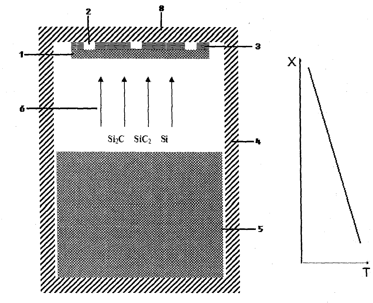
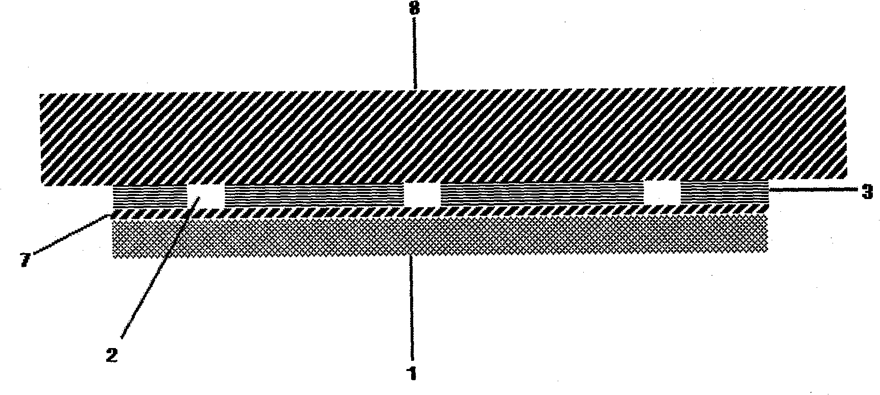
[0020] Take 0.5ml of the organic mixture (the mass percentage of furan methanol and phenolic resin is 3:1), apply it evenly on the back of the seed crystal with a coater, the thickness of the coating is 1 μm, and place it at room temperature for 24 hours to cure. The wafer is then gently placed in the graphite crucible with the organic coating side up. Put the graphite crucible into the graphite furnace again, pump the gas to 10 -3After Pa, the temperature was raised to 1000°C at a rate of 500°C / h, and the temperature was kept constant for 2 hours. Then fill it with argon gas 0.6 atm, raise the temperature at 500°C / h to 1800°C, keep the temperature for 1 hour, and finally cool it down to room temperature at the rate of 1000°C / h. After 8 hours, the graphite furnace was opened, and the wafer was taken out. There was a uniform graphite coating on the back of the wafer with a thickness of 1 μm.
Embodiment 2
[0022] Take 5ml of the organic mixture (the mass percentage of furan methanol and phenolic resin is 1:1), apply it evenly on the back of the seed crystal with a coater, the thickness of the coating is 30 μm, and place it at 60°C for 2 hours to cure. The wafer is then gently placed in the graphite crucible with the organic coating side up. Put the graphite crucible into the graphite furnace again, pump the gas to 10 -3 After Pa, it was raised to 1200°C at a rate of 500°C / h, and the temperature was kept constant for 1 hour. Then fill it with argon gas 0.6 atm, raise the temperature to 2200°C at 500°C / h, keep the temperature for 0.5 hours, and finally cool down to room temperature at the rate of 1000°C / h. After 8 hours, the graphite furnace was opened, and the wafer was taken out. There was a uniform graphite coating on the back of the wafer, with a thickness of 30 μm.
Embodiment 3
[0024] Take 10ml of the organic mixture (the mass percentage of furan methanol and phenolic resin is 1:3), apply it evenly on the back of the seed crystal with a coater, the coating thickness is 100μm, and place it at 80°C for 1 hour to cure. The wafer is then gently placed in the graphite crucible with the organic coating side up. Put the graphite crucible into the graphite furnace again, pump the gas to 10 -3 After Pa, it was raised to 1500°C at a rate of 500°C / h, and the temperature was kept constant for 0.5 hours. Then fill it with argon gas 0.6 atm, and raise the temperature to 2300°C at 500°C / h, keep the temperature for 0.5 hours, and finally cool down to room temperature at the rate of 1000°C / h. After 8 hours, the graphite furnace was opened, and the wafer was taken out. There was a uniform graphite coating on the back of the wafer with a thickness of 100 μm.
[0025] It should be noted that although the organic mixture of furan methanol and phenolic resin is used as ...
PUM
| Property | Measurement | Unit |
|---|---|---|
| thickness | aaaaa | aaaaa |
Abstract
Description
Claims
Application Information
 - R&D Engineer
- R&D Manager
- IP Professional
- Industry Leading Data Capabilities
- Powerful AI technology
- Patent DNA Extraction
Browse by: Latest US Patents, China's latest patents, Technical Efficacy Thesaurus, Application Domain, Technology Topic, Popular Technical Reports.
© 2024 PatSnap. All rights reserved.Legal|Privacy policy|Modern Slavery Act Transparency Statement|Sitemap|About US| Contact US: help@patsnap.com


