Method for manufacturing intermediate P-type electrode of tunable resonant cavity enhanced detector

An enhanced and detector technology, which is applied in the manufacture of microstructure devices, techniques for producing decorative surface effects, decorative arts, etc., can solve the problems of reduced corrosion selection ratio, difficult corrosion process, and increased production costs, to achieve Improve the corrosion selection ratio, reduce the difficulty and cost of the process, and improve the effect of P-type electrode contact

Inactive Publication Date: 2011-01-05
INST OF SEMICONDUCTORS - CHINESE ACAD OF SCI
View PDF4 Cites 5 Cited by
  • Summary
  • Abstract
  • Description
  • Claims
  • Application Information

AI Technical Summary

Problems solved by technology

For the general method, the P-type electrode is usually directly deposited on this layer of Al x Ga 1-x On the cut-off layer of As, the Al composition must be reduced to achieve high doping, but reducing the Al composition will make the sacrificial layer GaAs and the cut-off layer Al x Ga 1-x The As etching selectivity ratio decreases, and the general method uses dry etching to increase the etching selectivity ratio as much as possible, which brings difficulties to the etching process and increases the production cost

Method used


Image

  • Method for manufacturing intermediate P-type electrode of tunable resonant cavity enhanced detector
  • Method for manufacturing intermediate P-type electrode of tunable resonant cavity enhanced detector
  • Method for manufacturing intermediate P-type electrode of tunable resonant cavity enhanced detector

Examples


Embodiment Construction

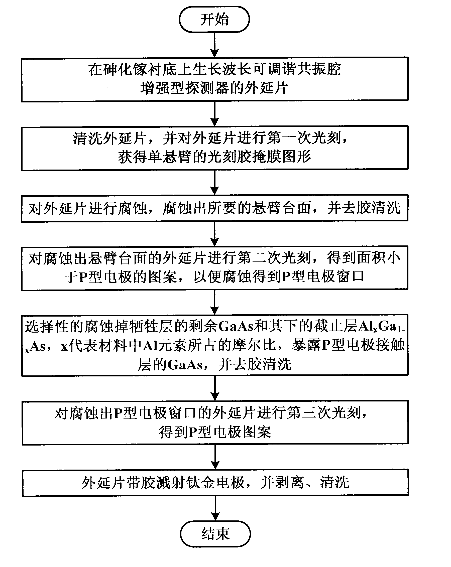
[0035] In order to make the object, technical solution and advantages of the present invention clearer, the present invention will be described in further detail below in conjunction with specific embodiments and with reference to the accompanying drawings.

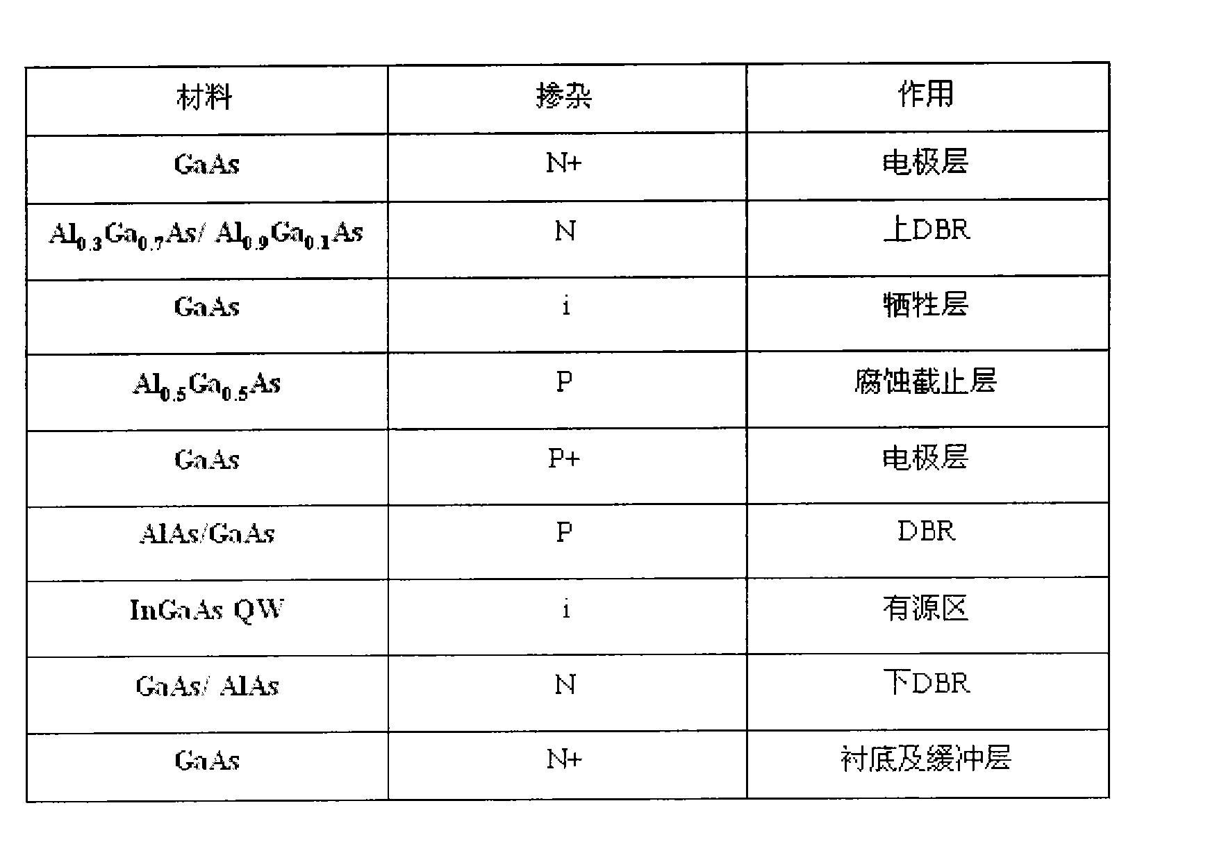
[0036] In the present invention, by rationally designing the material structure of the epitaxial wafer, the electrode contact layer is placed under the corrosion cut-off layer, and the corrosion cut-off layer adopts Al with a larger corrosion selection ratio. 0.5 Ga 0.5 As material, the electrode contact layer is made of GaAs material that can obtain higher P-type doping, and with two selective etching solutions, it solves the problem of making the intermediate P-type electrode.

[0037] like figure 1 as shown, figure 1 It is a flowchart of a method for making a P-type electrode in the middle of a tunable resonant cavity enhanced detector provided by the present invention, and the method includes:

[0038] A. Growth of...


PUM


Abstract

The invention discloses a method for manufacturing an intermediate P-type electrode of a tunable resonant cavity enhanced detector, which comprises the following steps of: growing an epitaxial wafer of the wavelength tunable resonant cavity enhanced detector on a gallium arsenide substrate; cleaning the epitaxial wafer, and performing primary photo-etching on the epitaxial wafer to obtain a photoresist mask graph of a single cantilever; corroding the epitaxial wafer to obtain an expected cantilever mesa, and performing glue removal and cleaning; performing secondary photo-etching on the epitaxial wafer where the cantilever mesa is corroded to obtain a pattern of which the area is smaller than that of the P-type electrode; selectively corroding the rest GaAs of a sacrificial layer and a stop layer AlxGa1-xAs below the sacrificial layer, exposing the GaAs of a contact layer of the P-type electrode, and performing glue removal and cleaning; performing third photo-etching on the epitaxial wafer where a P-type electrode window is corroded to obtain a P-type electrode pattern; and sputtering a titanium electrode on the epitaxial wafer with glue, and peeling and cleaning the electrode. The method solves the restriction condition between the stop layer and electrode contact layer materials, reduces the process difficulty and cost, and manufactures the excellent P-type electrode.

Description

technical field [0001] The invention relates to the field of micro-opto-electromechanical system (MOEMS) processing technology, in particular to a method for manufacturing a P-type electrode in the middle of a wavelength tunable resonant cavity enhanced detector. Background technique [0002] The current communication field is developing towards high-speed and high-capacity optical communication technology and all-optical communication network. Dense Wavelength Division Multiplexing (DWDM) system has become a key technology for long-distance optical signal transmission, which requires accurate monitoring of wavelength. MOEMS wavelength tunable filters, MOEMS wavelength tunable detectors and MOEMS wavelength tunable vertical cavity surface emitting lasers and other optoelectronic devices can effectively select and control wavelengths, and are used in high-speed and high-capacity optical communication technology and all-optical communication network technology has broad applic...

Claims


Application Information

Patent Timeline
IPC IPC(8): B81C1/00
Inventor 王杰韩勤杨晓红王秀平刘少卿
Owner INST OF SEMICONDUCTORS - CHINESE ACAD OF SCI
Why Eureka
Try Eureka