
Polycrystalline silicon texturing method

A technology of polycrystalline silicon wafer and acid texturing

Active Publication Date: 2010-11-03
EGING PHOTOVOLTAIC TECHNOLOGY CO LTD
View PDF1 Cites 32 Cited by
  • Summary
  • Abstract
  • Description
  • Claims
  • Application Information

AI Technical Summary

Problems solved by technology

It is unscientific to use the same acidic system to simultaneously remove the damaged layer and the textured treatment method in one acid corrosion method, and it is impossible to completely remove the damaged layer and obtain the ideal textured effect
[0006] For example, in the tank-type texturing, the circulating cooling method is adopted, and the liquid is pumped at the bottom of the tank, and the top of the tank overflows to complete the cycle, resulting in a relatively low temperature of the solution at the bottom of the silicon wafer and a relatively high temperature at the upper part, so that the temperature between different wafers and the same Different parts of a wafer are unevenly textured, which affects the textured effect
In addition, a large number of wafers are fed at one time, resulting in a relatively slow cooling rate. Since the temperature of the silicon wafer surface rises rapidly during the texturing process, and the surface temperature is relatively high, it is difficult to effectively remove the Ideal surface texturing while damaging the layer

Method used


Image

  • Polycrystalline silicon texturing method
  • Polycrystalline silicon texturing method
  • Polycrystalline silicon texturing method

Examples


specific Embodiment approach

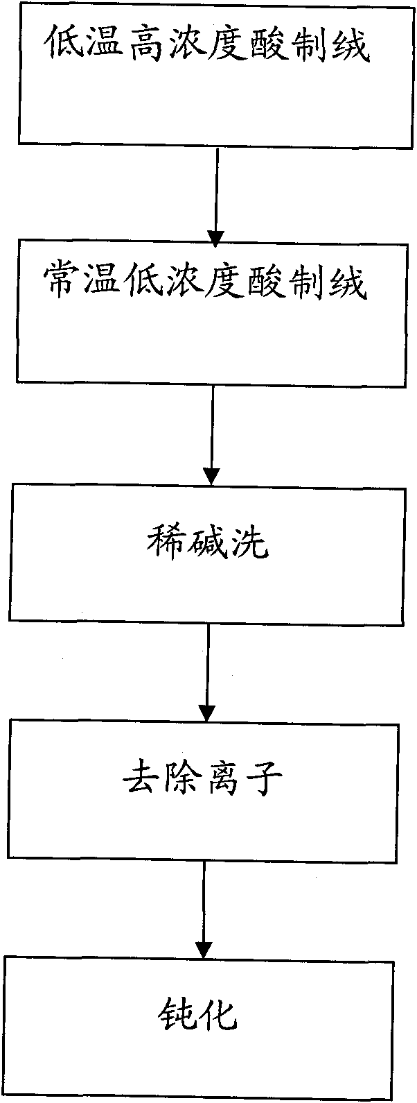
[0025]A polycrystalline silicon wafer texturing method, comprising the following steps: low-temperature high-concentration acid texturing, normal-temperature low-concentration acid texturing, dilute alkali washing, ion removal and passivation, the low-temperature high-concentration acid texturing and normal temperature low The acid treatment solution used in the high-concentration acid texture is a mixed acid solution of nitric acid, hydrofluoric acid and pure water.

[0026] The first step is low-temperature high-concentration acid velvet. The acid treatment solution used is a mixed acid solution of nitric acid with a mass fraction of 55%-65%, hydrofluoric acid with a mass fraction of 40%-55%, and pure water. Among them, nitric acid (HNO 3 ) volume fraction of 40%-60%, hydrofluoric acid (HF) volume fraction of 10%-25%, pure water (H 2 The volume fraction of O) is 15%-50%. Under the condition of 0.1MPa air pressure and circulating cooling, the liquid temperature is controlled...

Embodiment 1

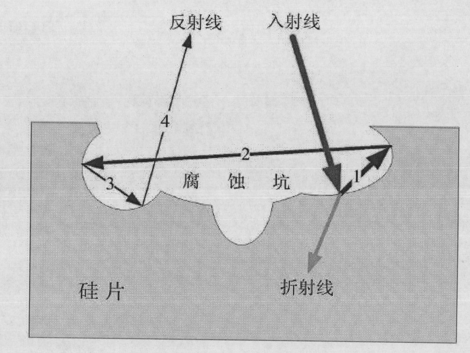
[0030] In the low-temperature high-concentration acid texturing process, the nitric acid (HNO 3 ) and hydrofluoric acid (HF) and pure water (H 2 The volume fractions of O) are 46.5%, 18.6%, and 34.9%, respectively. The polycrystalline silicon chip is immersed in the above-mentioned mixed acid solution at a temperature of 15°C. 3 The nitrogen gas per hour is disturbed, and the etching process is carried out for 80 seconds, and a slightly wider shallow etching pit (about 5um in width) is formed on the surface of the silicon wafer, (see Figure 4 ), the grain boundary corrosion is shallow, there is no obvious color difference between grains, no flower basket printing, and the available reflectance is 28.01% (see Figure 6 As shown in the middle curve 2), the surface damage layer can be effectively removed, the surface recombination of the battery can be reduced, and the surface light absorption is less.

[0031] In the normal temperature low-concentration acid texturing process,...

Embodiment 2

[0033] The first step is low-temperature and high-concentration acid velvet making. Nitric acid (HNO 3 ), hydrofluoric acid (HF) and pure water (H 2 The volume fraction of O) is 56.9%, 20.3%, and 22.8% respectively. The polysilicon wafer is immersed in the above-mentioned acidic treatment solution with a temperature of 8°C. 3 Under the condition of nitrogen perturbation per hour and the cooling device turned on for 50 seconds, the corrosion pits on the surface of the silicon wafer are shallow, the grain boundary corrosion is shallow, there is no obvious color difference between the grains, no flower basket printing, and the surface damage layer is effectively removed. Reduce battery surface recombination.

[0034] The second step is to make texture with low-concentration acid at room temperature. Wash the silicon wafers treated in the first step and immerse them in the acidic treatment solution for texturing, in which nitric acid (HNO 3 ), hydrofluoric acid (HF) and pure w...


PUM

PropertyMeasurementUnit
reflectanceaaaaaaaaaa

Abstract

The invention discloses a polycrystalline silicon texturing method which comprises low-temperature high-concentration acidizing fluid texturing, normal-temperature low-concentration acidizing fluid, alkali cleaning, ion removal and passivation. The invention provides more a proper acid treatment fluid and a corrosion texturing process for the polycrystalline silicon texturing to ensure that the removal of a mechanical damage layer on the surface of a silicon slice and the texturing are easier to control, can accurately control the texturing degree of the surface of the silicon slice and the thickness reduction of the silicon slice, shorten the texturing time, improve the texturing yield of a battery, reduce the surface reflectivity, increase the light absorption and the short-circuit current, and improve the photo-electricity conversion efficiency of the battery.

Description

【Technical field】 [0001] The invention relates to the manufacturing technology of solar cells, in particular to the texturing technology of polycrystalline silicon wafers. 【Background technique】 [0002] In recent years, polycrystalline silicon solar cells have been more and more widely used due to their high conversion efficiency, stable performance and moderate cost, and their output has surpassed that of monocrystalline silicon, occupying a dominant position in the market. [0003] In order to improve the photoelectric conversion efficiency of solar cells, it is necessary to chemically treat the silicon wafer during production, so that the surface of the silicon is made into a suede surface with a certain shape. Due to the existence of the suede surface, the reflectivity of the surface of the object will be greatly reduced. , thereby increasing light absorption. The texturing of polycrystalline silicon wafers is isotropic etching on the surface of silicon wafers through ...

Claims


Application Information

Patent Timeline
Patent Type & Authority Applications(China)
IPC IPC(8): C30B33/10C23F1/24H01L31/18
CPCY02P70/50
Inventor 屈莹
Owner EGING PHOTOVOLTAIC TECHNOLOGY CO LTD
Learn More