Metal oxide thin film transistor and preparation method thereof

A technology for oxide thin films and transistors, which is used in transistors, semiconductor/solid-state device manufacturing, semiconductor devices, etc. to improve interface contact, increase process difficulty, and reduce off-state current.

Inactive Publication Date: 2010-10-27
SOUTH CHINA UNIV OF TECH
View PDF3 Cites 18 Cited by
  • Summary
  • Abstract
  • Description
  • Claims
  • Application Information

AI Technical Summary

Problems solved by technology

[0006] In order to simultaneously improve the contact characteristics between the insulating layer and the metal oxide layer, the source-drain electrode (Ni) and the metal oxide layer, and improve the electrical stability of the device, the metal oxide transition layer with high oxygen content and the insulating layer have Good interface contact, the metal oxide semiconductor layer with low oxygen content has good interface contact with metal nickel, which can significantly improve the electrical performance of thin film transistors using metal nickel as source and drain electrode materials; wherein low oxygen content The metal oxide layer mainly plays the role of semiconductor; the electrical properties of the high-oxygen metal oxide layer are between semiconductor and insulator, and it mainly plays a transition role. The transition layer can improve the interface contact between the semiconductor layer and the insulating layer, reduce charge defects at the interface, thus reducing the off-state current (I off ), improve electron mobility, improve current switch ratio (I on / I off ), improve the electrical performance of the transistor

Method used


Image

  • Metal oxide thin film transistor and preparation method thereof
  • Metal oxide thin film transistor and preparation method thereof
  • Metal oxide thin film transistor and preparation method thereof

Examples


Embodiment 1

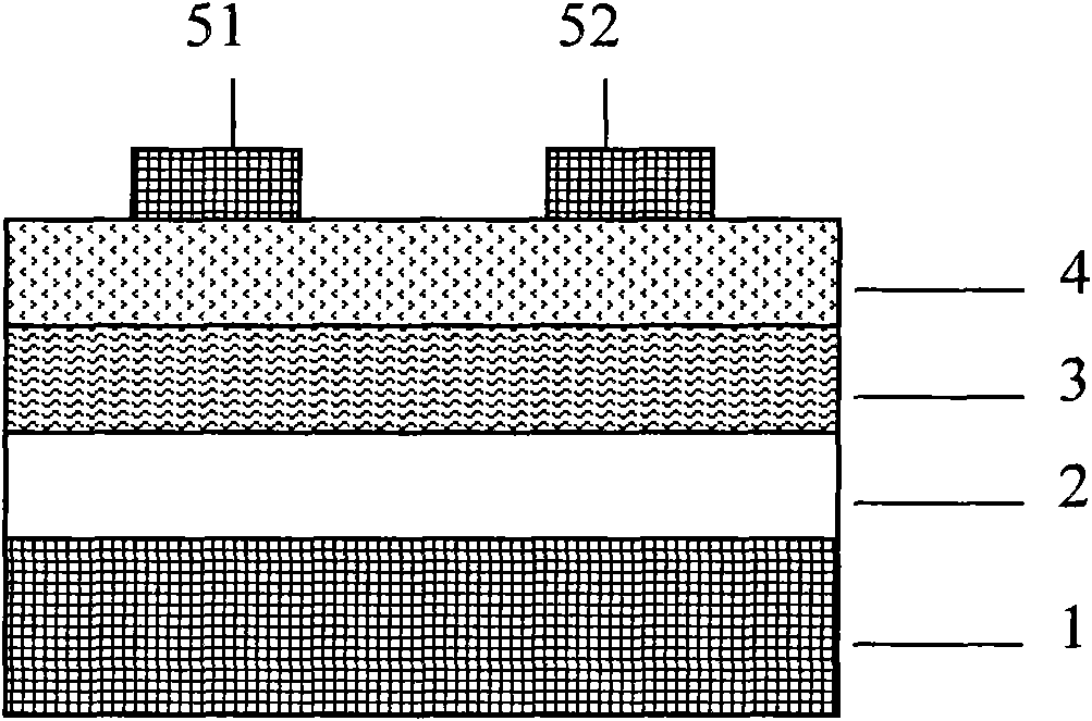
[0030] Use a highly doped silicon wafer as the gate 1, thermally oxidize a layer of silicon dioxide with a thickness of 300nm on it as the insulating layer 2, and measure its permittivity C i 11.4nF / cm 2 .

[0031] The transition layer 3 is prepared on the insulating layer 2 by radio frequency (RF) sputtering, and the target used for sputtering is indium gallium zinc oxide (InGaZnO), where In 2 o 3 , Ga 2 o 3 The molar ratio of ZnO and ZnO is 1:1:2; the theoretical value content of oxygen calculated by the molar ratio is (x=1, y=1, z=2): [(3x+3y+z) / (5x+ 5y+2z)]=[(3+3+2) / (5+5+4)]=57.1%; Oxygen (O 2 ) flow is 25SCCM, the flow of argon (Ar) is 10SCCM, O 2 / Ar=2.5; the sputtering power is 100W, and a high oxygen content indium gallium zinc oxide (InGaZnO) film with a thickness of 5nm is obtained.

[0032] The semiconductor layer 4 is prepared on the transition layer 3 by radio frequency (RF) sputtering. The target material used for sputtering is also indium gallium zinc oxi...


PUM


Abstract

The invention discloses a metal oxide thin film transistor and a preparation method thereof. The metal oxide thin film transistor is composed of a grid electrode, an insulating layer, a transition layer, a semiconductor layer, a drain electrode and a source electrode, wherein the grid electrode, the insulating layer, the transition layer and the semiconductor layer are sequentially connected with each other from bottom to top; the drain electrode and the source electrode are positioned on the semiconductor layer; the transition layer and the semiconductor layer are prepared by means of sputtering with the same target being adopted in the process of sputtering, the material of the target is (In2O3)x(Ga2O3)y(ZnO)z, wherein x, y and z are not less than 0 but not more than 1, and x+y+z is equal to 1; and the transition layer and the insulating layer include excellent contact property so as to effectively lower carrier trap density between contact interfaces of the insulating layer and the transition layer as well as enhance output current of the transistor and improve electrical stability. The source electrode and the drain electrode can form outstanding ohmic contact with the semiconductor layer, thereby effectively reducing off-state current, raising on / off ratio of current and improving electronic carrier mobility.

Description

technical field [0001] The invention relates to a thin film transistor, in particular to a metal oxide thin film transistor and a preparation method thereof. The thin film transistor is mainly used for active driving of organic light emitting display, liquid crystal display and electronic paper, and can also be used for integrated circuits. Background technique [0002] In recent years, thin film transistors based on metal oxides have attracted more and more attention because of their advantages such as high mobility, good light transmission, stable film structure, low preparation temperature and low cost. The main goal of the development of metal oxide thin film transistors is to be used in flat panel displays, flexible electronic devices, transparent electronic devices, and sensors. In terms of flat panel display, thin film transistors made of materials such as hydrogenated amorphous silicon (a-Si:H) or polysilicon are currently mainly used. However, the limitations of hyd...

Claims


Application Information

Patent Timeline
IPC IPC(8): H01L29/786H01L29/12H01L21/34H01L21/363
CPCH01L21/02554H01L29/7869H01L21/02565H01L21/02631H01L29/517
Inventor 彭俊彪兰林锋徐苗徐瑞霞王磊许伟
Owner SOUTH CHINA UNIV OF TECH
Why Eureka
Try Eureka