Technological method for preparing Cr-doped beta-FeSi2 films

A process method and thin-film technology, applied in metal material coating technology, ion implantation plating, coating, etc., can solve the problems that the thin film does not have semiconductor properties, it is difficult to control the content of impurities in the thin film, and achieve the reduction of lattice parameters Effect

Inactive Publication Date: 2010-07-21
GUIZHOU UNIV
View PDF2 Cites 4 Cited by
  • Summary
  • Abstract
  • Description
  • Claims
  • Application Information

AI Technical Summary

Problems solved by technology

[0004] The technical problem to be solved by the present invention is to provide a method for preparing Cr-doped β-FeSi 2 Thin-film process methods to overcome the shortcomings of the existing technology that it is difficult to control the content of impurities in the film, or the formed film does not have semiconductor properties, etc.

Method used


Image

  • Technological method for preparing Cr-doped beta-FeSi2 films
  • Technological method for preparing Cr-doped beta-FeSi2 films
  • Technological method for preparing Cr-doped beta-FeSi2 films

Examples


Embodiment Construction

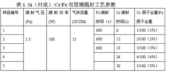
[0024] Embodiment of the present invention: implementing the technical solution of the present invention, using Si (substrate) / Cr / Fe double-layer film structure to prepare Cr-doped β-FeSi 2 The process of the thin film is as follows: the substrate adopts a p-Si (100) single wafer polished on one side, and the resistivity is 7-13 . Before the substrate Si chip was loaded into the sample chamber, it was ultrasonically cleaned in acetone, absolute ethanol, and deionized water for 10 minutes each, and washed with a diluted HF solution (HF:H 2 O=1:50) Soak for 30s-1min, rinse with deionized water, and use N 2Blow it dry, put it into the sampling chamber, and backsplash for 8-10 minutes to further clean the Si chip. The cleaned Si sheet is sent into the sputtering chamber through the magnetic transfer rod, and the preliminary vacuum is drawn to 2×10 -5 Pa.

[0025] Pass the working gas Ar gas into the sputtering chamber, adjust the sputtering pressure to 2.0Pa and maintain this...


PUM

PropertyMeasurementUnit
thicknessaaaaaaaaaa
band gapaaaaaaaaaa

Abstract

The invention discloses a technological method for preparing Cr-doped beta-FeSi2 films on the basis of a magnetron sputtering method. The technological method comprises the following steps: firstly, rinsing a Si sheet; secondly, depositing a Cr/Fe or Fe/Cr double-layer film or a Fe/Cr/Fe multi-layer film on the substrate of the Si sheet by using the magnetron sputtering method, wherein the content of Cr is controlled by regulating the sputtering rate of each layer and the thickness of the film layer, so that the content of Cr substituting Fe is 1% to 5%; and thirdly, annealing the Cr/Fe or Fe/Cr double-layer film or the Fe/Cr/Fe multi-layer film deposited by using the magnetron sputtering method in a vacuum annealing furnace, so as to obtain the Cr-doped beta-FeSi2 film. According to the XRD (X-ray diffraction) measurement, the crystal structure of beta-FeSi2 is not changed by doping.

Description

technical field [0001] The invention relates to a method for preparing β-FeSi 2 Thin film technology. Background technique [0002] Low Temperature Stable Phase β-FeSi in Transition Metal Silicide Fe-Si Compounds 2 It is a new type of semiconductor material, which is composed of Fe and Si elements that are extremely abundant on the earth. Even if it is used for a long time, it is non-toxic and harmless to the human body and the environment. Its processing and preparation process has no load on the environment, so it is called environmentally friendly. semiconductors. β-FeSi 2 It also has a series of excellent properties, such as its preparation method is compatible with the existing silicon-based microelectronics process, it is considered to be a quasi-direct band gap material, and its band gap value is about 0.83-0.87eV, corresponding to the characteristics of modern optical communication frequency range, with a high light absorption coefficient (>10 5 cm -1 ), has...

Claims


Application Information

Patent Timeline
Patent Type & Authority Applications(China)
IPC IPC(8): C23C14/35C23C14/16C23C14/02
Inventor 谢泉张晋敏肖清泉梁艳曾武贤王衍马道京
Owner GUIZHOU UNIV
Why Eureka
Try Eureka