


Quick Research
Generate reliable direction feasibility study reports for your R&D in just a few steps.

Technical Q&A
Discover and master advanced knowledge NOW. Basics, ideas, possibilities, all at once.

Find Solutions
As an expert in R&D theories, this can generate solutions to your technical problems instantly.

Evaluate Feasibility
Analyze your overall solution with one click, know your potential R&D risks in advance.

Monitor Landscape
Get weekly tech updates, stay abreast of the latest tech innovations and key insights.
Storage device drive method
A driving method and technology of a storage device, which are applied in information storage, static memory, digital memory information, etc., can solve the problems of difficulty in improving reliability, damage to variable resistance elements, increase current of variable resistance elements, etc., and achieve data retention. The effect of stabilization of operation, avoidance of diffusion and disappearance, and improvement of reliability
- Summary
- Abstract
- Description
- Claims
- Application Information
AI Technical Summary
Problems solved by technology
Method used
Image

Examples
no. 1 approach
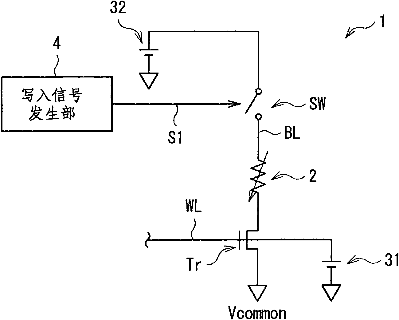
[0027] figure 1 An example of the circuit configuration of the memory cell 1 in the memory device to which the memory device driving method of the first embodiment of the present invention is applied is shown. The memory cell 1 includes: a variable resistance element 2; a selection transistor Tr; a gate voltage source 31; a switch SW; a write voltage source 32; In addition, a storage device (memory) is constituted by arranging a plurality of memory cells 1 having such a configuration in a matrix, for example.
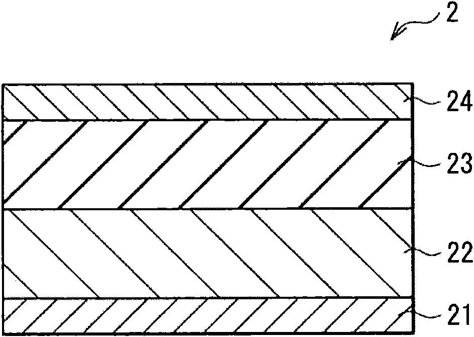
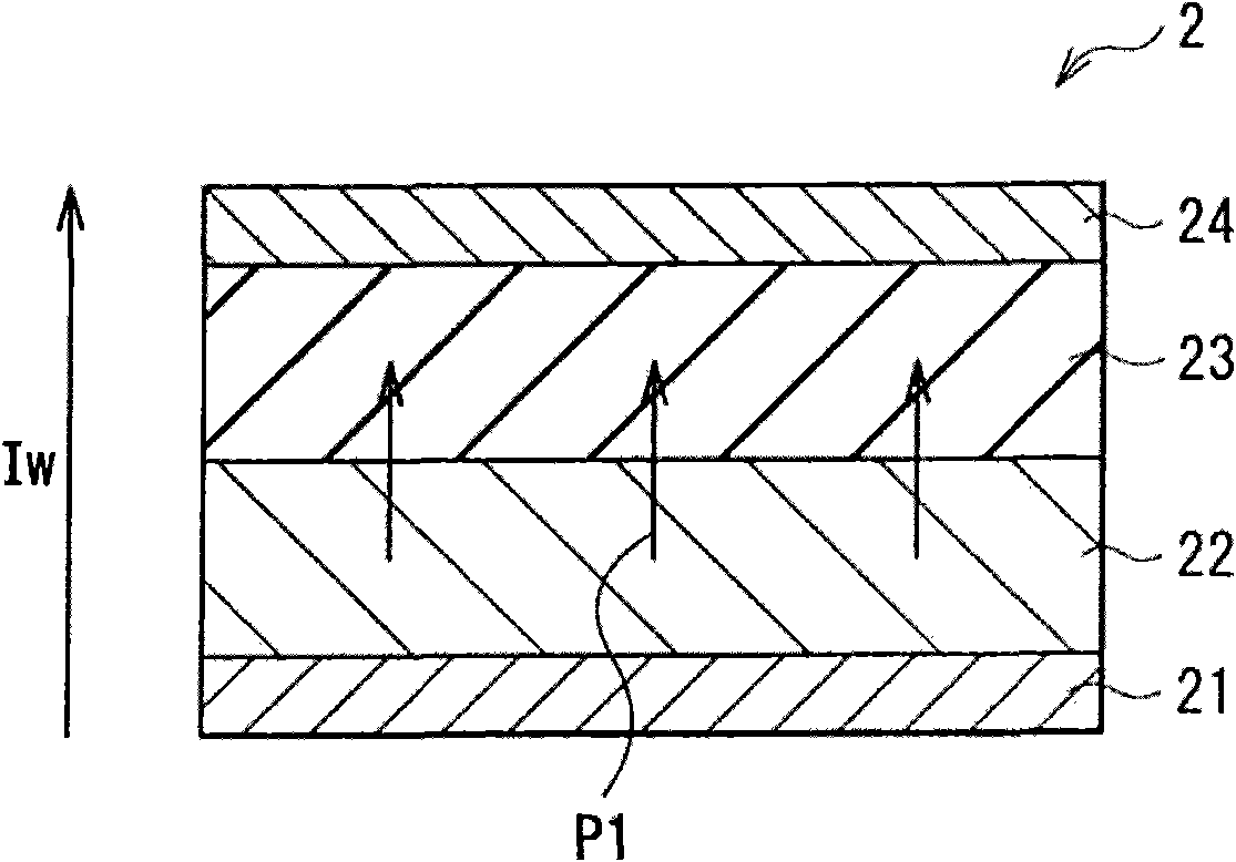
[0028] The variable resistance element 2 has a pair of electrodes described later, and can reversibly change the resistance value by applying voltages of different polarities (writing voltage and erasing voltage described later) between the pair of electrodes . In addition, the detailed structure of this variable resistance element 2 will be described later.
[0029] The gate of the selection transistor Tr is connected to a selection word line (selection word line) W...
no. 2 approach
[0051] Next, a second embodiment of the present invention will be described. In addition, the same elements as those in the first embodiment are denoted by the same reference numerals, and thus explanations are appropriately omitted.
[0052] Figure 8 An example of the data writing method of this embodiment is shown, specifically, a timing waveform at the time of the data writing operation is shown. In addition, since the storage device to which the data writing method of this embodiment is applied is the same as that described in the first embodiment, description thereof will be omitted.
[0053] Here, first, before describing the data writing method of this embodiment, the details of the data writing operation will be considered. It can be considered that this data writing operation consists of two stages. First, in the first stage, a write voltage is applied between the electrodes 21, 24 in the high-resistance state of the insulating characteristic, and a soft breakdown...
PUM
 Abstract
Description
Claims
Application Information
 - R&D Engineer
- R&D Manager
- IP Professional
- Industry Leading Data Capabilities
- Powerful AI technology
- Patent DNA Extraction
Browse by: Latest US Patents, China's latest patents, Technical Efficacy Thesaurus, Application Domain, Technology Topic, Popular Technical Reports.
© 2024 PatSnap. All rights reserved.Legal|Privacy policy|Modern Slavery Act Transparency Statement|Sitemap|About US| Contact US: help@patsnap.com