Light-emitting element

A technology of light-emitting components and semiconductors, applied in the direction of electrical components, semiconductor devices, circuits, etc.

Active Publication Date: 2010-06-16
EPISTAR CORP
View PDF0 Cites 8 Cited by
  • Summary
  • Abstract
  • Description
  • Claims
  • Application Information

AI Technical Summary

Problems solved by technology

Figure 1B It is a schematic diagram of the energy gap (bandgap) and light-emitting mechanism of known light-emitting diodes, such as Figure 1B As shown, since the carrier mobility of the hole h is smaller than that of the electron e, it is known that the electron e and the hole h in the light-emitting diode 100 are often only closer to the p-type semiconductor layer 120 Therefore, in the active layer 122, the light-emitting regions are concentrated near the several quantum well layers 126 near the p-type semiconductor 124, causing only a few structures in the active layer 122 to emit light.

Method used


Image

  • Light-emitting element
  • Light-emitting element
  • Light-emitting element

Examples


Embodiment Construction

[0029] Embodiments of the present invention are described below with reference to the accompanying drawings.

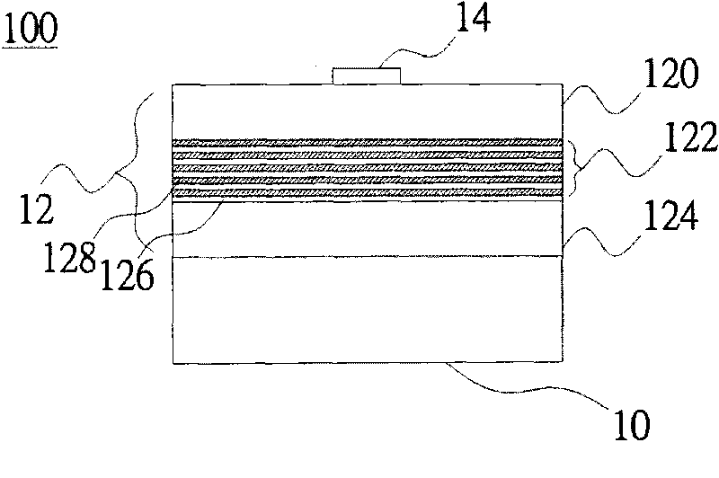
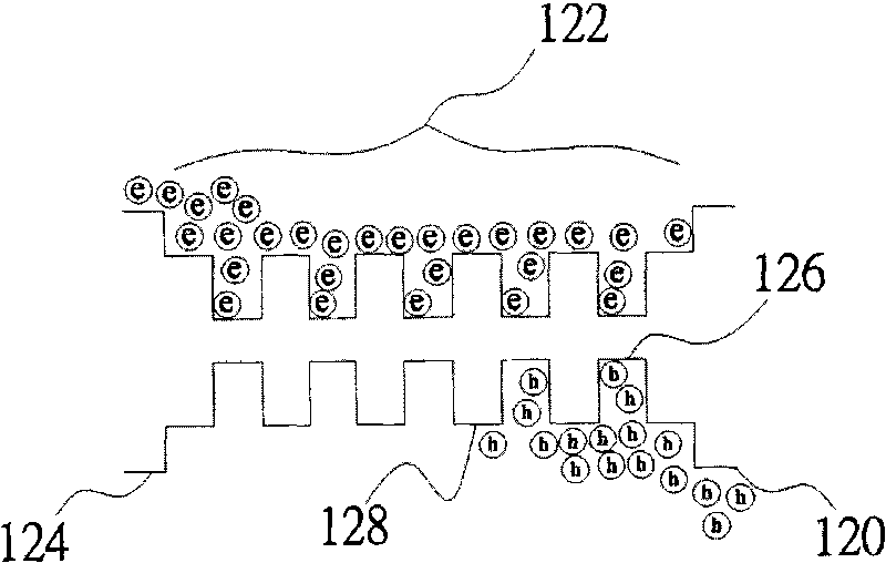
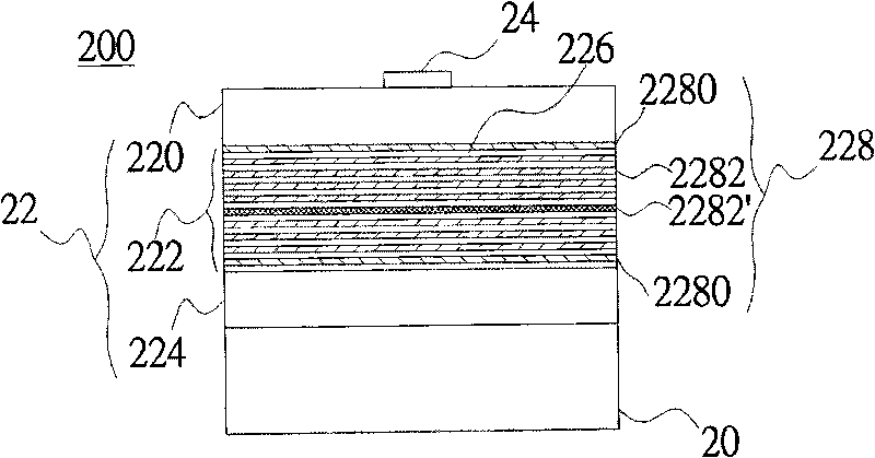
[0030] figure 2 and image 3 It is a structural schematic diagram of an embodiment of the present invention. Such as figure 2 As shown, the light-emitting element 200 includes a substrate 20, a semiconductor stack 22 on the substrate 20, and at least one electrode 24 on the semiconductor stack 22, wherein the above-mentioned substrate 20 can be an insulating, conductive, transparent or light-absorbing substrate, and its material It can be metal, zinc oxide (ZnO), silicon carbide (SiC), sapphire (sapphire), silicon (silicon), gallium arsenide (GaAs) or gallium phosphide (GaP), and the above-mentioned semiconductor stack 22 The material can be selected from III / V semiconductor materials including aluminum (Al), gallium (Ga), indium (In), phosphorus (P), arsenic (As) or nitrogen (N), such as gallium nitride (GaN ) series materials, aluminum gallium indium phosphide...


PUM


Abstract

The invention mainly aims at disclosing a light-emitting element which comprises a semiconductor stack, wherein the semiconductor stack comprises an active layer, the active layer is in a multiple quantum well (MQW) structure formed by stacking a plurality of quantum well layers and a plurality of barrier layers in a staggered manner, and the plurality of the barrier layers comprise at least one doped barrier layer and one undoped barrier layer. Therefore, the doped barrier layer can improve the carrier mobility of a hole, uniformize a light-emitting region in the active layer and improve the internal quantum efficiency (IQE) of the light-emitting element.

Description

technical field [0001] The present invention relates to a light-emitting device structure, in particular to a light-emitting device with at least one doped barrier layer and one undoped barrier layer in the active layer. Background technique [0002] A light-emitting diode (light-emitting diode, LED) is a widely used light source in optoelectronic components. Compared with traditional incandescent bulbs or fluorescent tubes, light-emitting diodes have the characteristics of energy saving and long service life, so they gradually replace traditional light sources and are used in various fields, such as traffic signs, backlight modules, street lighting, medical equipment Wait. [0003] Figure 1A It is a schematic diagram of a known light-emitting element structure, such as Figure 1A As shown, the known light-emitting element 100 includes a substrate 10, a semiconductor stack 12 on the substrate 10, and an electrode 14 on the semiconductor stack 12, wherein the semiconductor ...

Claims


Application Information

Patent Timeline
Patent Type & Authority Applications(China)
IPC IPC(8): H01L33/00
Inventor 王俊凯洪详竣许育宾朱瑞溢吴欣显颜伟昱
Owner EPISTAR CORP
Why Eureka
Try Eureka