
IC (integrated circuit)-packaged wafer expanding device

A technology of outer ring and inner ring, applied in the direction of transportation and packaging, conveyor objects, electrical components, etc., can solve the problems of low production efficiency, inability to effectively realize mechanization and automation, and difficulty in quality assurance, and achieve high production efficiency, The effect of high degree of mechanization and automation and ingenious design

Inactive Publication Date: 2010-06-16
GUANGDONG UNIV OF TECH
View PDF0 Cites 13 Cited by
  • Summary
  • Abstract
  • Description
  • Claims
  • Application Information

AI Technical Summary

Problems solved by technology

The disadvantages of the existing crystal expansion device are that the process of supplying the outer ring and the inner ring, taking the chip and the process of expanding the crystal cannot be effectively mechanized and automated, the production efficiency is low, and the quality is difficult to guarantee

Method used


Image

  • IC (integrated circuit)-packaged wafer expanding device
  • IC (integrated circuit)-packaged wafer expanding device
  • IC (integrated circuit)-packaged wafer expanding device

Examples


Embodiment

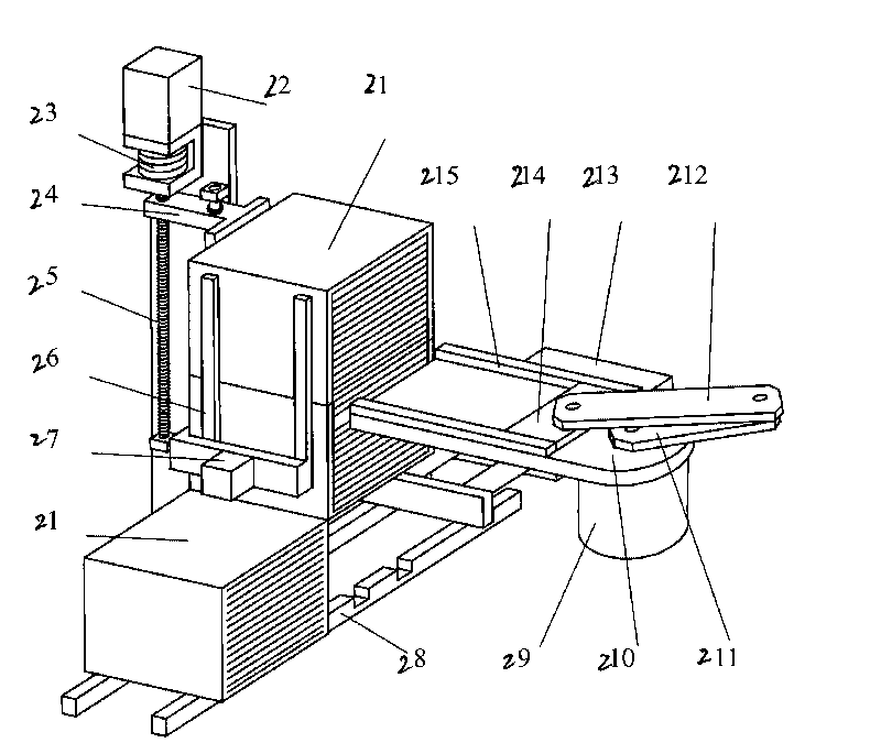
[0026] The schematic diagram of the film box feeding mechanism and the taking-up principle of the present invention is as follows: figure 2 As shown, the silicon wafer is fixed in the liner 9 by the adhesive film, and is stored in the sheet box 21. There are many grids in the chip box 21, and each silicon wafer is inserted in a separate grid and isolated from each other, and the chips are protected during transportation and access. Sheet cassettes 21 are stacked in the sheet cassette station that support 26 and landing gear 24 etc. constitute. Landing gear 24 is restrained by parts such as linear guide rail, nut and screw mandrel 25, and under the drive of stepper motor 22, screw mandrel 25 rotates, and landing gear 24 moves up and down along linear guide rail. Each time, the sheet cassette 21 moves one grid from top to bottom, and then moves down one grid after the sheet taking mechanism takes out a silicon wafer. When a sheet cassette 21 has been supplied, the grid of the...


PUM


Abstract

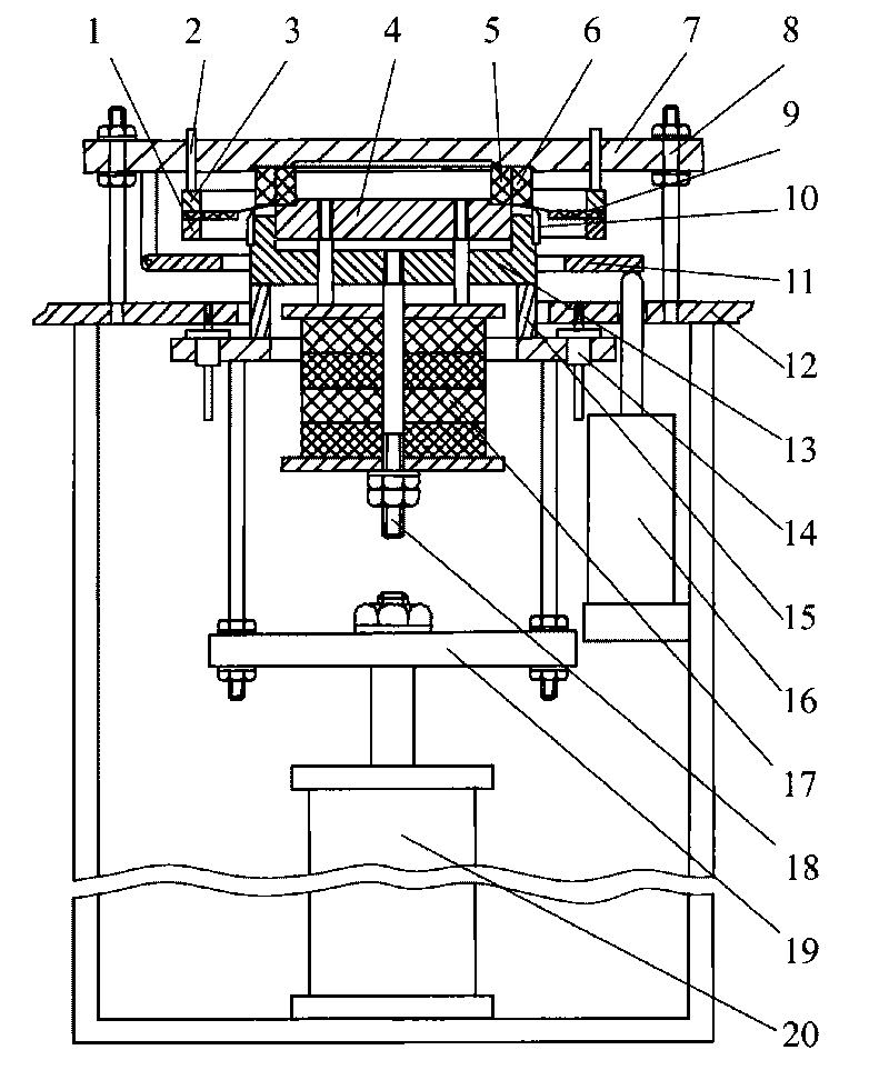
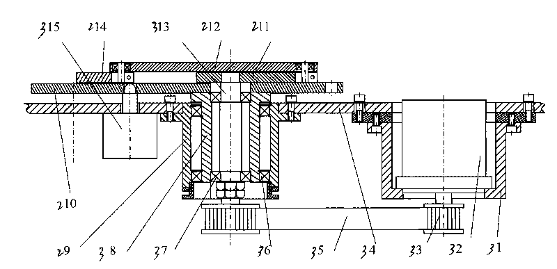
The invention relates to an IC (integrated circuit)-packaged wafer expanding device which comprises a wafer box feeding mechanism, a wafer picking mechanism, a wafer expanding mechanism and the like. In the wafer box feeding mechanism, a screw rod rotates and an undercarriage drives a wafer box to descend grid by grid under the driving of a stepping motor; the wafer box stops for a period of time for each one-grid descent so that the wafer picking mechanism can take a wafer from a wafer disc; and when the feeding of one wafer box is finished, a new wafer box is fed sequentially. The wafer picking mechanism is powered by only one electric motor to finish the whole wafer picking, wafer transferring and wafer delivering processes by being matched with the operation of an electric magnet. In the wafer expanding mechanism, the inner ring of a wafer can be pressed into the outer ring with the middle clamped with a rubber film, so that the silicon wafer can be tightened, thereby finishing the operation of tightening the inner ring and the outer ring. The process is powered by a main air cylinder. When the inner ring is pressed into the outer ring and placed in position, a piston rod of the main air cylinder moves upwards sequentially, a serrated knife contacts the tightened rubber film, a serrated tip punctures the rubber film, and a crevasse is torn towards the direction between two teeth, thereby enabling a liner frame to be separated from the expanded wafer. The invention can realize the mechanization and the automation, has high production efficiency, and can ensure the production quality.

Description

technical field [0001] The invention relates to an IC encapsulating crystal encapsulating device for encapsulating a finished wafer in an IC manufacturing process to form a usable wafer on a chip bonder, and belongs to the transformation technology of an IC encapsulating encapsulating crystal encapsulating device. Background technique [0002] The production of IC components is divided into the pre-process of chip manufacturing and the post-process of microelectronic packaging. The previous process is generally to melt the polycrystalline silicon and pull out the monocrystalline silicon ingot, and then cut it into thin monocrystalline silicon wafers, that is, wafers. After grinding, polishing, photolithography and other processes, hundreds of thousands of integrated circuits are made on a wafer. [0003] The post-process is the microelectronic packaging process, including: chip bonding, wire bonding, plastic packaging, testing, sorting, marking, etc., and finally can produc...

Claims


Application Information

Patent Timeline
Patent Type & Authority Applications(China)
IPC IPC(8): H01L21/00H01L21/50H01L21/677
Inventor 李克天王晓临刘吉安欧阳祥波
Owner GUANGDONG UNIV OF TECH
Learn More