Dual side cooling integrated power device package and module and methods of manufacture

A technology for integrating power and molding materials, which is applied in semiconductor/solid-state device components, semiconductor devices, electrical components, etc., and can solve the problem that the module footprint is not the footprint

Inactive Publication Date: 2010-03-24
FAIRCHILD SEMICON CORP
View PDF6 Cites 5 Cited by
  • Summary
  • Abstract
  • Description
  • Claims
  • Application Information

AI Technical Summary

Problems solved by technology

[0009] While the integrated transistor modules of the latter disclosed patent publication are useful for the intended application, the module footprint is not typical in the industry

Method used


Image

  • Dual side cooling integrated power device package and module and methods of manufacture
  • Dual side cooling integrated power device package and module and methods of manufacture
  • Dual side cooling integrated power device package and module and methods of manufacture

Examples


Embodiment Construction

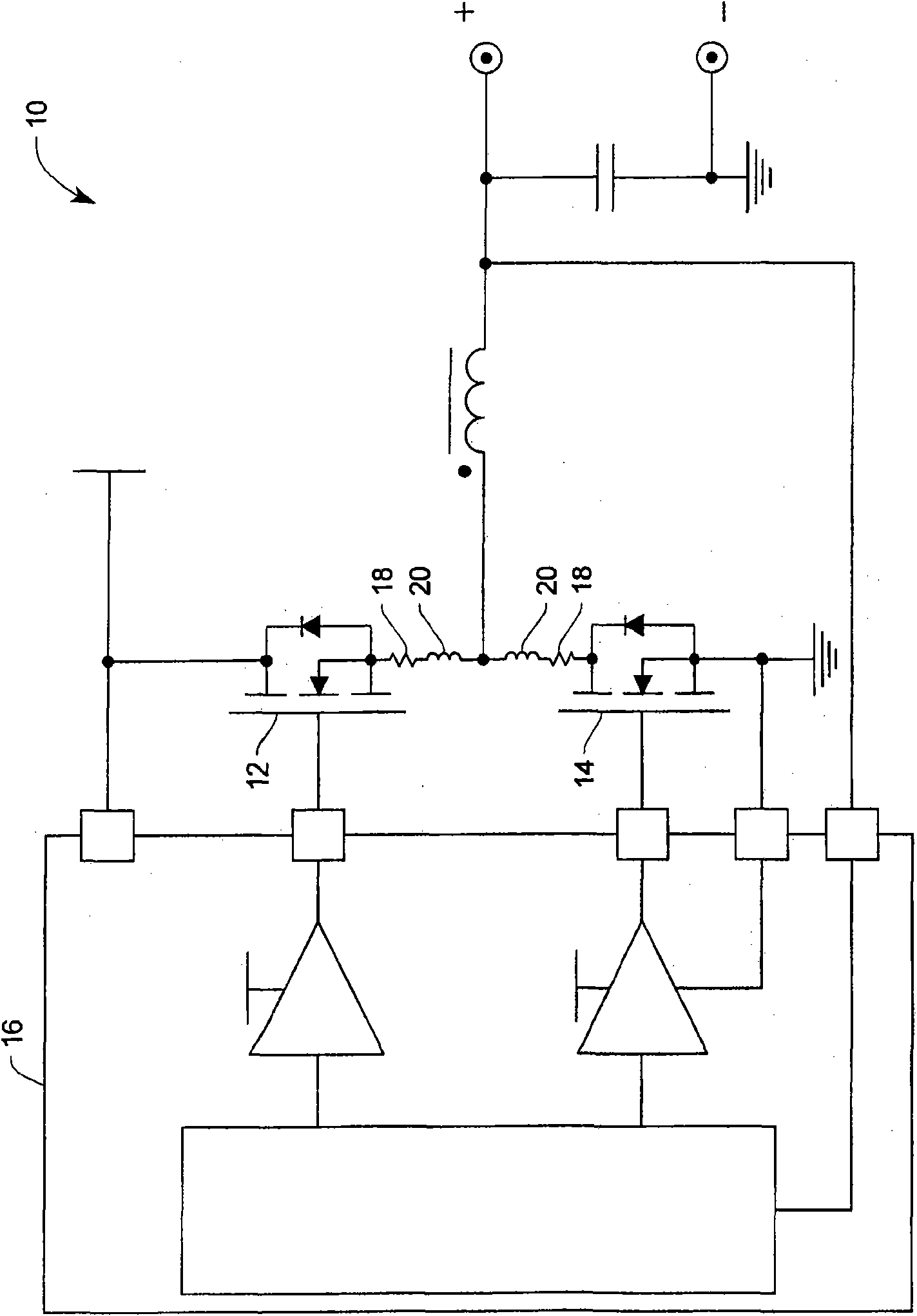
[0056] Embodiments of the invention are directed to semiconductor die packages and methods for manufacturing semiconductor die packages. A semiconductor die package according to an embodiment of the present invention includes a substrate and a semiconductor die mounted on the substrate. The semiconductor die may be attached to the substrate using an adhesive or any other suitable attachment material. In semiconductor die packaging, the bottom surface and / or the top surface of the semiconductor die may be electrically coupled to conductive regions of the substrate. The encapsulation material may encapsulate the semiconductor die. As will be explained in further detail below, substrates according to embodiments of the invention may have different configurations in different embodiments.

[0057] The substrate may have any suitable configuration. However, in a preferred embodiment of the invention said substrate comprises a lead frame structure and a molding material. Typical...


PUM


Abstract

An integrated power device module having a leadframe structure with first and second spaced pads and one or more common source-drain leads located between said first and second pads, first and secondtransistors flip chip attached respectively to said first and second pads, wherein the source of said second transistor is electrically connected to said one or more common source-drain leads, and a first clip attached to the drain of said first transistor and electrically connected to said one or more common source-drain leads. In another embodiment a partially encapsulated power quad flat no-lead package having an exposed top thermal drain clip which is substantially perpendicular to said with a folded stud exposed top thermal drain clip, and an exposed thermal source pad.

Description

[0001] Cross References to Related Applications [0002] This application claims priority to US Patent Application Serial No. 11 / 829,793, filed July 27,2007. technical field [0003] The present invention relates generally to the packaging of semiconductor devices and, more particularly, to double side cooled integrated power device modules and methods of manufacturing the same. Background technique [0004] Small packages for semiconductors with short leads are desirable for forming compact electronic circuits. However, such small packages create problems in dissipating heat from packaged power devices used in electronic circuits. In many cases, the heat dissipation capabilities of the leads alone are not sufficient to provide reliable operation of the power device. In the past, heat sinks have been attached to such devices to help dissipate heat. [0005] Another factor in forming compact circuits is the amount of space required for wire bonding in conventional package...

Claims


Application Information

Patent Timeline
Patent Type & Authority Applications(China)
IPC IPC(8): H01L23/42
CPCH01L2924/01027H01L23/49524H01L24/36H01L23/3107H01L2224/83385H01L2224/16245H01L2224/73253H01L2924/01015H01L2224/16H01L24/39H01L2224/32057H01L23/49548H01L2924/01047H01L2924/01046H01L2924/01078H01L2924/01006H01L23/36H01L24/48H01L24/40H01L2924/01079H01L23/49575H01L23/49562H01L2924/14H01L2224/32245H01L2224/73255H01L2924/01024H01L2924/01005H01L2924/01082H01L2924/01013H01L2924/13091H01L2224/49171H01L2924/30107H01L2924/014H01L24/49H01L2924/01029H01L2224/48247H01L2924/01033H01L2224/37147H01L24/37H01L2224/05554H01L2224/40245H01L2224/40095H01L2924/1306H01L2924/1305H01L2924/181H01L2924/00H01L2924/00012H01L2924/00014H01L2224/84801H01L2224/83801H01L24/84H01L2224/45099H01L2224/45015H01L2924/207H01L2224/73221H01L23/42
Inventor 乔纳森·A·诺奎尔鲁宾·马德里
Owner FAIRCHILD SEMICON CORP
Why Eureka
Try Eureka