Method for preparing vanadium dioxide thin film with high temperature coefficient of resistance

A technology of vanadium dioxide and temperature coefficient, which is applied in the manufacture of circuits, electrical components, and final products, can solve the problems of high material noise, unfavorable device integration process, and limited detector performance, and achieve a firm combination

Inactive Publication Date: 2010-01-13
HUAZHONG UNIV OF SCI & TECH
View PDF0 Cites 13 Cited by
  • Summary
  • Abstract
  • Description
  • Claims
  • Application Information

AI Technical Summary

Problems solved by technology

The TCR of polysilicon and vanadium oxide is not much different, but the former needs to be processed at a high temperature of nearly 1000 °C, which is very unfavorable to the integration process of the device
The superconductor YBCO has a high TCR, but the noise of the material is large, and the performance of the detector is limited; although the noise of the metal is very small, its TCR is only 1 / 10 of that of vanadium oxide, and it is difficult to obtain high-performance devices

Method used


Image

  • Method for preparing vanadium dioxide thin film with high temperature coefficient of resistance
  • Method for preparing vanadium dioxide thin film with high temperature coefficient of resistance
  • Method for preparing vanadium dioxide thin film with high temperature coefficient of resistance

Examples


Embodiment Construction

[0020] Below by embodiment the present invention will be further described:

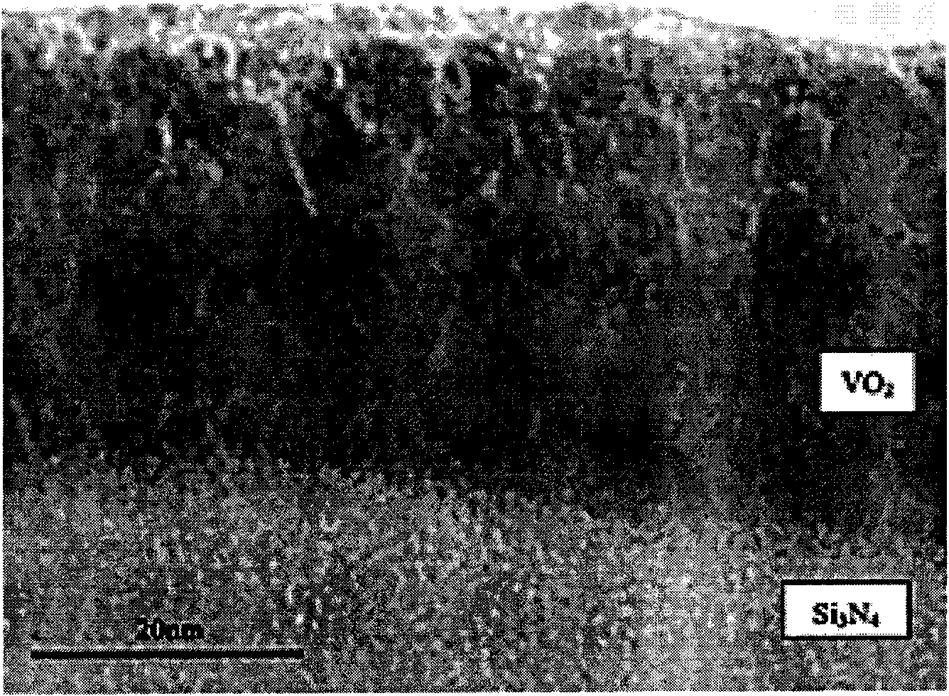
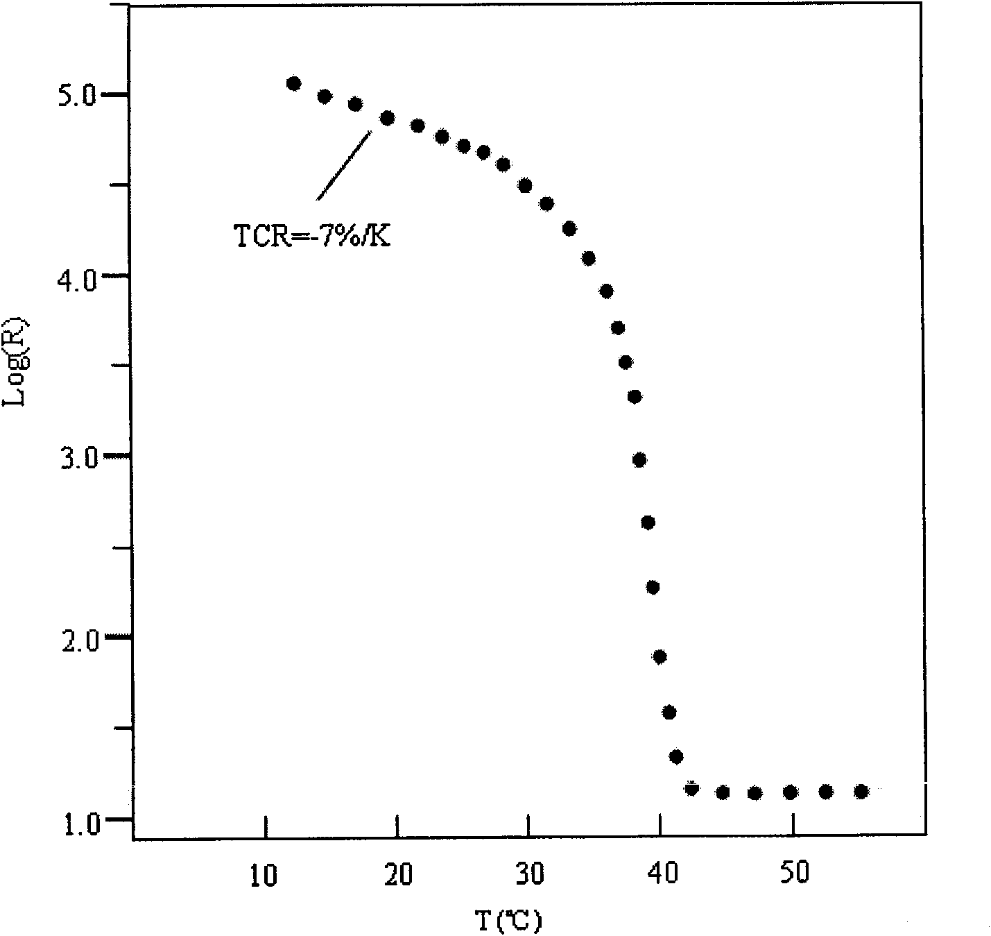
[0021] 1. VO with a temperature coefficient of resistance of -7% / K 2 Film Preparation Process

[0022] (1) Clean the substrate of the high-resistance silicon with (100) crystal orientation according to the standard RCA process, and then dry it with nitrogen.

[0023] (2) Put the silicon wafer into the reactive ion sputtering system, turn on the heating device, and keep the substrate temperature at 280°C; after the vacuum degree reaches the required substrate temperature and stabilizes, clean the surface of the silicon wafer by parallel ion beam sputtering. The sputtering uses a vanadium target with a purity of 4N, the purity of the sputtering reaction gas is 4N, and the deposition rate is 2-3nm / min. The process parameters are as follows:

[0024]

[0025] (3) Use the focused ion source to clean the surface of the sputtering target for 3 minutes, and then open the baffle to sputter the buffer la...


PUM

PropertyMeasurementUnit
Temperature coefficient of resistanceaaaaaaaaaa

Abstract

The invention discloses a method for preparing a vanadium dioxide thin film with high temperature coefficient of resistance, which can be used for uncooled infrared detection. The method comprises the following steps: on a silicon substrate on which Si3N4 thin film or SiO2 thin film is deposited, a vanadium oxide thin film which is 50-200nm thick is deposited by using a reactive ion bean sputtering method; after the thin film is naturally cooled, sample wafers are taken out, and annealing is then performed. The thin film prepared using the method of the invention has a nanometer structure with 5-20nm of average crystalline grain, and has appropriate square resistance with temperature coefficient of resistance (TCR) from -5% / K to -7% / K in semiconductor region; in addition the prepared thin film has as equivalent noise level as the common nanometer structure vanadium dioxide. Therefore, the vanadium dioxide thin film is quite a potential uncooled infrared detection material.

Description

technical field [0001] The invention belongs to thin film preparation technology, and in particular relates to a preparation method of a high-performance vanadium dioxide thin film used for an uncooled infrared detector. Background technique [0002] The uncooled infrared focal plane array (IR-UFPA) realizes night vision and related applications by receiving infrared radiation emitted by objects. Compared with photon-type detectors, it does not need to be cooled to 77K by liquid nitrogen, but works at room temperature, which makes it have the advantages of low cost, light weight, low power consumption, and easy maintenance, which greatly promotes the development of this technology. Devices for both military and civilian markets. At the same time, the requirements for high-performance UFPA are becoming more and more intense. [0003] The temperature resistance coefficient (TCR) of the thermally sensitive material of UFPA device and the noise of the material itself are the m...

Claims


Application Information

Patent Timeline
IPC IPC(8): H01L31/18C23C14/34C23C14/10C23C14/08C23C14/06
CPCY02P70/50
Inventor 赖建军何少伟戴君易新建
Owner HUAZHONG UNIV OF SCI & TECH
Why Eureka
Try Eureka