Low damage ICP etching method for manufacturing GaN base photoelectric device
A photoelectric device, low-damage technology, applied in the direction of electrical components, semiconductor devices, semiconductor/solid-state device manufacturing, etc., can solve problems such as complex processes and long time consumption, to ensure production efficiency, improve stability and reliability, and improve production Effects on efficiency and product quality
- Summary
- Abstract
- Description
- Claims
- Application Information
AI Technical Summary
Problems solved by technology
Method used
Image
Examples
Embodiment 1
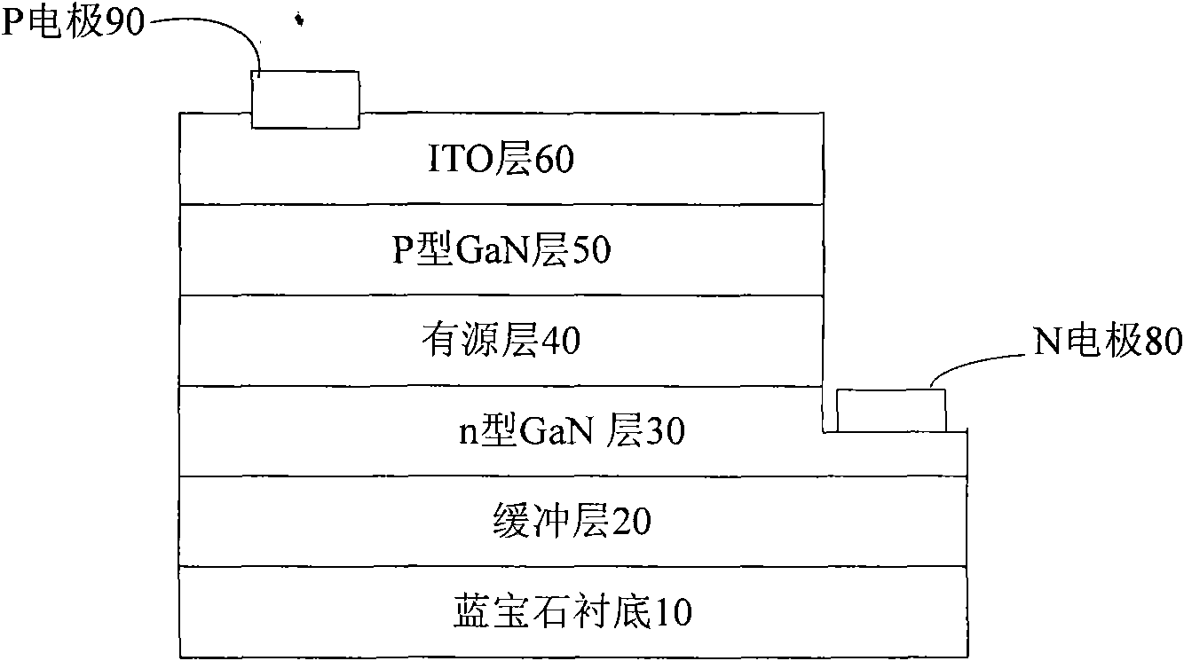
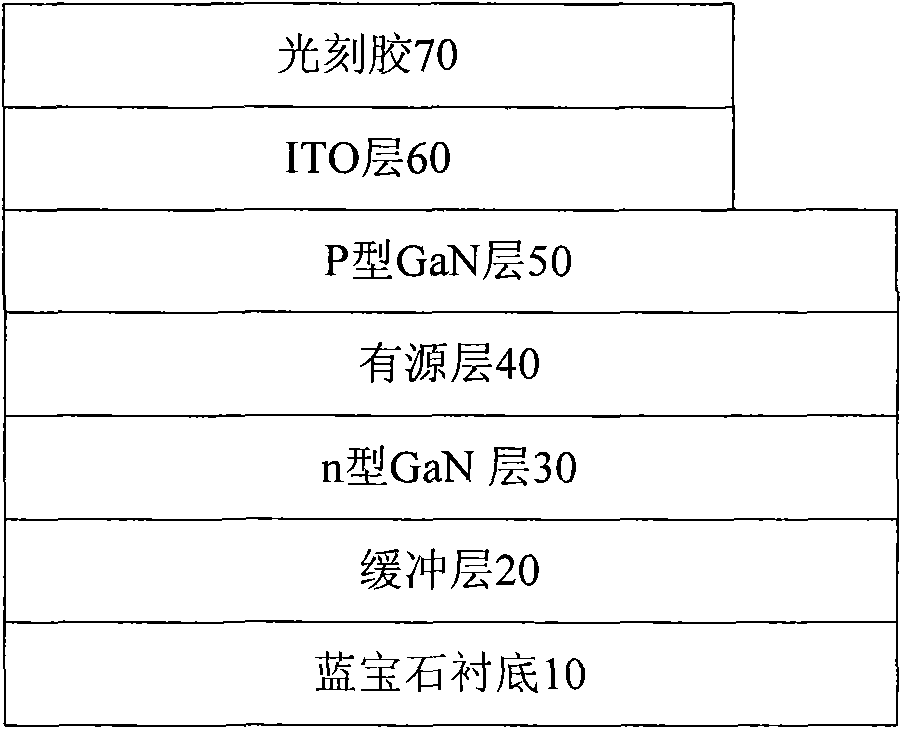
[0024] Please refer to figure 2 As shown, it is a schematic cross-sectional view of the GaN-based light-emitting diode prepared in this embodiment. When preparing the GaN-based light-emitting diode, conventional production equipment and process methods in the field can be used to sequentially epitaxial buffer layer 20, n-type GaN layer 30, active layer 40 and p-type GaN layer 50 on sapphire substrate 10 to form GaN The material structure of the base LED; then, a layer of ITO (indium tin oxide) layer 70 is prepared on the surface of the p-type GaN layer 50 by means of electron beam evaporation or sputtering; then a layer of photoresist 80 is coated on its surface. , using photolithography technology to expose the ITO on a part of the p-type GaN layer 50, the thickness of the photoresist is 1.5-3um, this embodiment is preferably 2um; then wet etching is used to etch away the previously exposed ITO, and the exposed part is p-type GaN, such as Figure 3a shown.
[0025] Using ...
Embodiment 2
[0032] Please refer to figure 2 As shown, it is a schematic cross-sectional view of the GaN-based light-emitting diode prepared in this embodiment. When preparing the GaN-based light-emitting diode, conventional production equipment and process methods in the field can be used to sequentially epitaxial buffer layer 20, n-type GaN layer 30, active layer 40 and p-type GaN layer 50 on sapphire substrate 10 to form GaN The material structure of the base LED; then, a layer of ITO (indium tin oxide) layer 70 is prepared on the surface of the p-type GaN layer 50 by means of electron beam evaporation or sputtering; then a layer of photoresist 80 is coated on its surface. , using photolithography technology to expose the ITO on a part of the p-type GaN layer 50, the thickness of the photoresist is 1.5-3um, this embodiment is preferably 2um; then wet etching is used to etch away the previously exposed ITO, and the exposed part is p-type GaN, such as Figure 3a shown.
[0033] Using ...
Embodiment 3
[0040] Please refer to figure 2 As shown, it is a schematic cross-sectional view of the GaN-based light-emitting diode prepared in this embodiment. When preparing the GaN-based light-emitting diode, conventional production equipment and process methods in the field can be used to sequentially epitaxial buffer layer 20, n-type GaN layer 30, active layer 40 and p-type GaN layer 50 on sapphire substrate 10 to form GaN The material structure of the base LED; then, a layer of ITO (indium tin oxide) layer 70 is prepared on the surface of the p-type GaN layer 50 by means of electron beam evaporation or sputtering; then a layer of photoresist 80 is coated on its surface. , using photolithography technology to expose the ITO on a part of the p-type GaN layer 50, the thickness of the photoresist is 1.5-3um, this embodiment is preferably 2um; then wet etching is used to etch away the previously exposed ITO, and the exposed part is p-type GaN, such as Figure 3a shown.
[0041] Using ...
PUM
 Abstract
Description
Claims
Application Information
 - R&D
- Intellectual Property
- Life Sciences
- Materials
- Tech Scout
- Unparalleled Data Quality
- Higher Quality Content
- 60% Fewer Hallucinations
Browse by: Latest US Patents, China's latest patents, Technical Efficacy Thesaurus, Application Domain, Technology Topic, Popular Technical Reports.
© 2025 PatSnap. All rights reserved.Legal|Privacy policy|Modern Slavery Act Transparency Statement|Sitemap|About US| Contact US: help@patsnap.com


