Forming method of 3D NAND storage
A 3D NAND and memory technology, which is applied in the direction of electric solid-state devices, semiconductor devices, electrical components, etc., can solve problems such as storage structure failure, and achieve the effects of preventing failure, preventing etching or damage, and slowing down the slope
- Summary
- Abstract
- Description
- Claims
- Application Information
AI Technical Summary
Problems solved by technology
Method used
Image
Examples
Embodiment Construction
[0031] As mentioned in the background, the existing multi-layer stacked 3D NAND memory has the problem of failure.
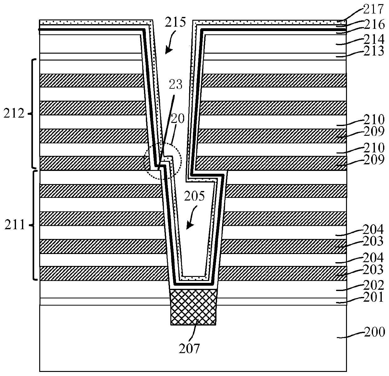
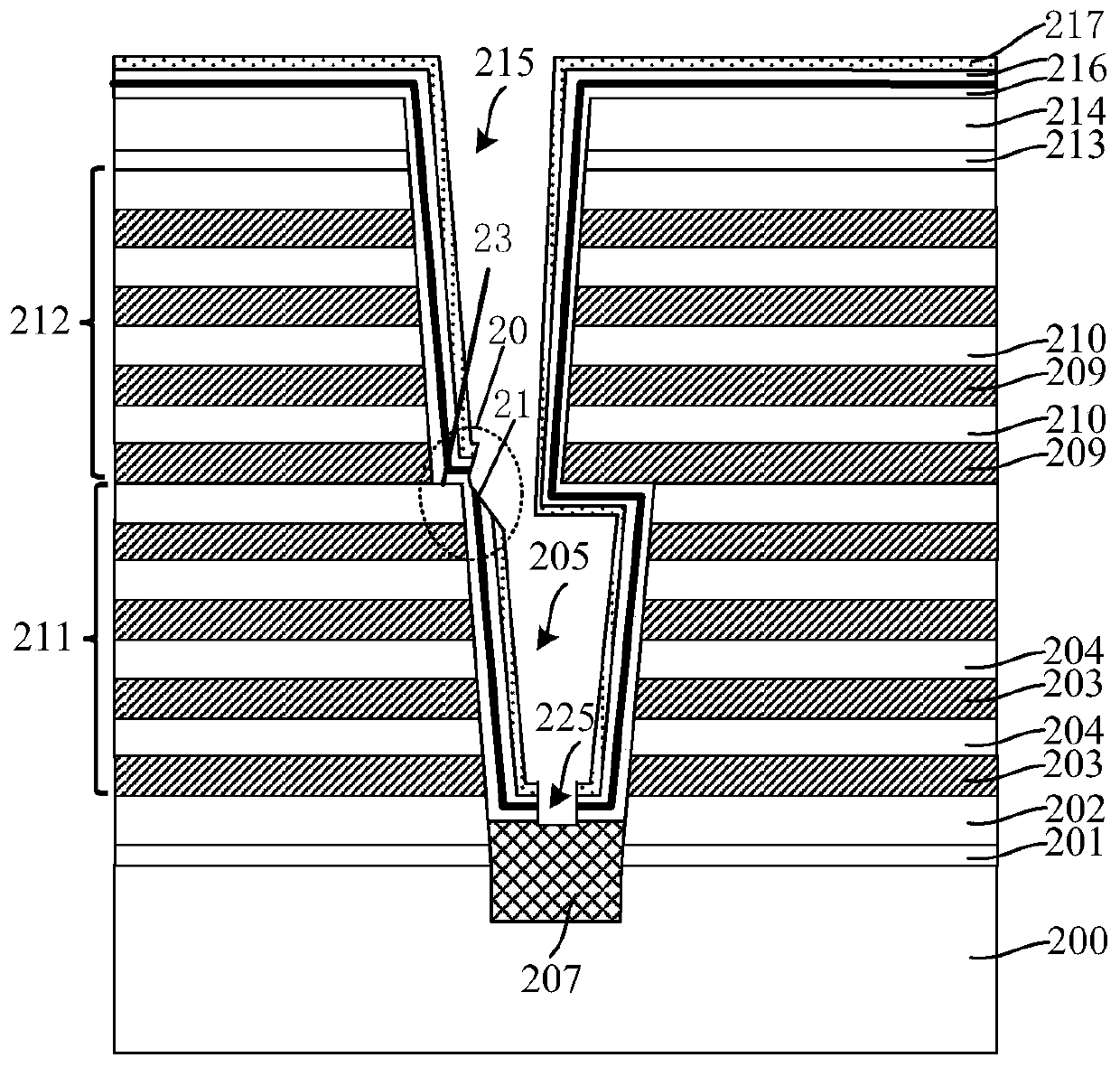
[0032] The study found that the location where the failure problem of multi-layer stacked 3D NAND memory generally occurs at the junction of the multi-layer stacked structure, please refer to figure 2 20 positions indicated by the dotted box in .
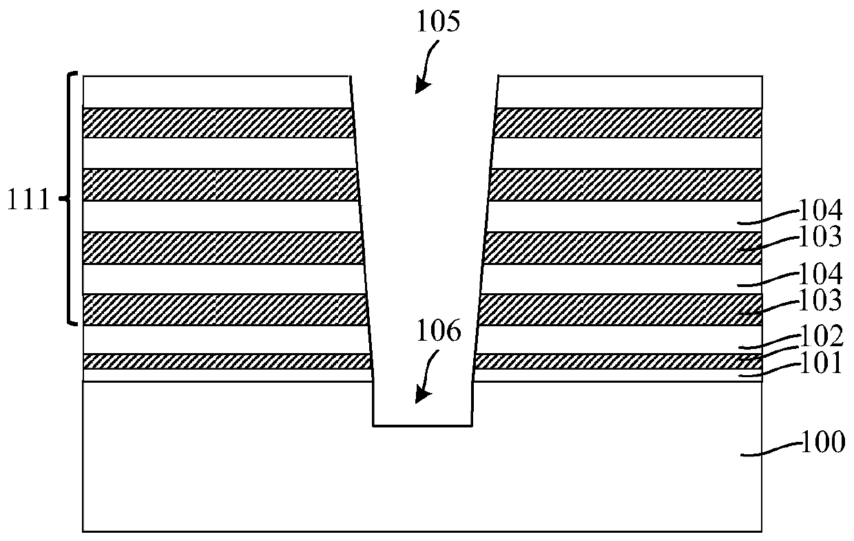
[0033] After further research, the specific reasons for the above problems are: Figure 1-2 It is a schematic diagram of the cross-sectional structure of the formation process of the 3D NAND memory according to an embodiment of the present invention. First, please refer to figure 1 , forming a first stack structure 211 on the semiconductor substrate 200, the first stack structure 211 includes a number of alternately stacked sacrificial layers 203 and insulating layers 204, the first stack structure 211 and the semiconductor substrate 200 can also be Form a buffer oxide layer 201 and a dielectric layer 202; etch th...
PUM
 Abstract
Description
Claims
Application Information
 - R&D
- Intellectual Property
- Life Sciences
- Materials
- Tech Scout
- Unparalleled Data Quality
- Higher Quality Content
- 60% Fewer Hallucinations
Browse by: Latest US Patents, China's latest patents, Technical Efficacy Thesaurus, Application Domain, Technology Topic, Popular Technical Reports.
© 2025 PatSnap. All rights reserved.Legal|Privacy policy|Modern Slavery Act Transparency Statement|Sitemap|About US| Contact US: help@patsnap.com


