
Method for preparing slot field-effect transistor with back-gate ZnO multi-nano wire

A manufacturing method and transistor technology, applied in the direction of nanostructure manufacturing, nanotechnology, nanotechnology, etc., can solve the problems of the gap, the small working current of ZnO nanowire field effect transistors, etc., and achieve the effect of increasing the current

Inactive Publication Date: 2009-09-23
INST OF MICROELECTRONICS CHINESE ACAD OF SCI
View PDF0 Cites 23 Cited by
  • Summary
  • Abstract
  • Description
  • Claims
  • Application Information

AI Technical Summary

Problems solved by technology

[0006] In order to solve the problem that the existing ZnO nanowire field effect transistor has a small working current and has a large gap with practical applications, the present invention provides a method for manufacturing a back gate ZnO multi-nanowire field effect transistor, using multiple ZnO nanowires as Parallel channels and suspend the nanowire channel in the air to improve the sensing performance of field effect transistors

Method used


Image

  • Method for preparing slot field-effect transistor with back-gate ZnO multi-nano wire
  • Method for preparing slot field-effect transistor with back-gate ZnO multi-nano wire

Examples


Embodiment Construction

[0027] The present invention will be described in further detail below in combination with specific embodiments and with reference to the accompanying drawings.

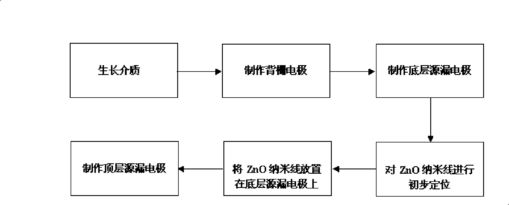
[0028] see figure 1 and figure 2 , a method for manufacturing a back gate ZnO multi-nanowire trench field effect transistor, the steps of the method are as follows:

[0029] (1) On the upper surface of the substrate 1, use RF plasma enhanced chemical vapor deposition technology PECVD to grow SiO 2 Dielectric 2 is used as a gate oxide dielectric;

[0030] (2) evaporating metal on the back side of the substrate 1 as the back gate electrode 3;

[0031] (3) Electrode metal is made on the upper surface of the substrate through steps such as photolithography, evaporation, and stripping, as the bottom source and drain electrodes 4;

[0032] (4) Using AC bidirectional dielectrophoresis technology to initially immobilize ZnO nanowires 5, the process is as follows: put the ZnO nanowire material into an isopropanol solutio...


PUM


Abstract

The invention discloses a method for preparing a slot field-effect transistor with a back-gate ZnO multi-nano wire, which belongs to the technical field of compound semiconductor materials and devices. The invention provides a method for preparing a slot field-effect transistor with back-gate ZnO multi-nano wire so as to solve the problem that the existing field effect transistor with back-gate ZnO nano wire has small working current which has large gap with practical applications; the method comprises the following steps of: growing medium, preparing a back-gate electrode, preparing a bottom source-drain electrode, fixing the ZnO nano wire primarily by using alternating current bi-directional dielectrophoresis technology, controlling the ZnO nano wire accurately by using nano controlling technology based on AFM, and preparing a top source-drain electrode. A plurality of ZnO nano wires are taken as parallel slots and suspended in the air, which can greatly improve the performance of current, transconductance, and cut-off frequency and the like of devices, and improve the performance of ultraviolet, gas and chemical sensing.

Description

technical field [0001] The invention relates to the technical field of compound semiconductor materials and devices, in particular to a method for manufacturing a back-gate ZnO multi-nanowire channel field effect transistor. Background technique [0002] ZnO is currently the material with the most abundant nanostructures and properties. The realized nanostructures include nanowires, nanobelts, nanorings, nanocombs, nanotubes, etc. Among them, due to the miniaturization of materials, the specific surface area of ​​one-dimensional nanowires increases, and has surface effects, small size effects, quantum effects and macroscopic quantum tunneling effects that conventional bulk materials do not have. The crystal quality is better, and the transport performance of carriers more superior. One-dimensional nanowires can not only realize basic nanoscale components (such as lasers, sensors, field effect transistors, light-emitting diodes, logic circuits, spintronic devices, and quantu...

Claims


Application Information

Patent Timeline
Patent Type & Authority Applications(China)
IPC IPC(8): H01L21/336B82B3/00
Inventor 徐静波付晓君张海英
Owner INST OF MICROELECTRONICS CHINESE ACAD OF SCI
Learn More