


Quick Research
Generate reliable direction feasibility study reports for your R&D in just a few steps.

Technical Q&A
Discover and master advanced knowledge NOW. Basics, ideas, possibilities, all at once.

Find Solutions
As an expert in R&D theories, this can generate solutions to your technical problems instantly.

Evaluate Feasibility
Analyze your overall solution with one click, know your potential R&D risks in advance.

Monitor Landscape
Get weekly tech updates, stay abreast of the latest tech innovations and key insights.
System and method for monitoring semiconductor processing technique
A technology of processing technology and monitoring system, applied in semiconductor/solid-state device testing/measurement, semiconductor/solid-state device manufacturing, electrical components, etc. Ratio and other issues to achieve the effect of improving signal-to-noise ratio and resolution, improving accuracy and reliability, and realizing precise control
- Summary
- Abstract
- Description
- Claims
- Application Information
AI Technical Summary
Problems solved by technology
Method used
Image

Examples
Embodiment 1
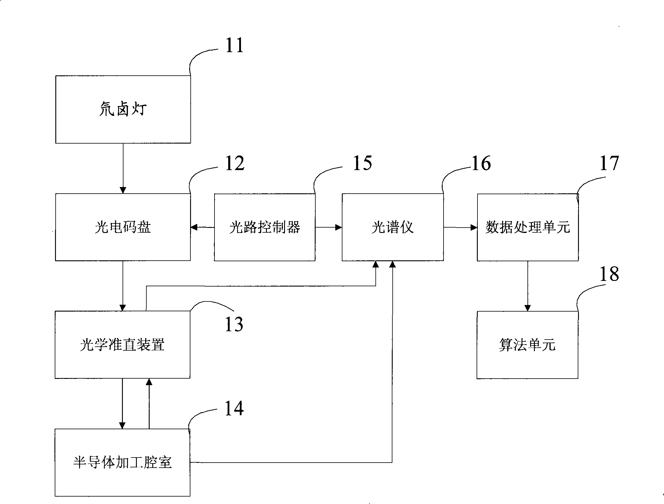
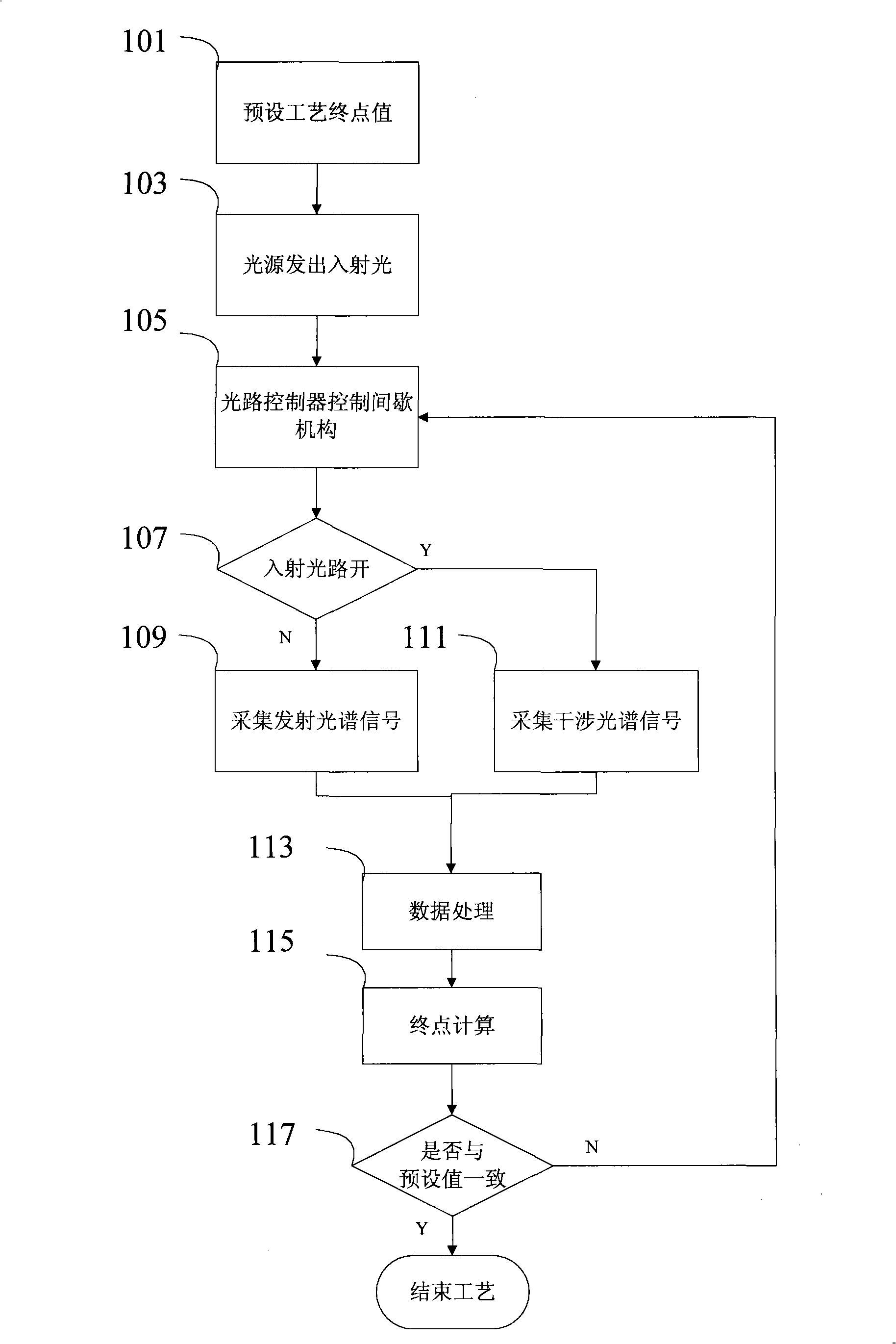
[0037] The present invention discloses a monitoring system and method for semiconductor processing technology, referring to figure 1 and figure 2 An embodiment of the present invention is described. figure 1 It is a schematic diagram of the monitoring system of the semiconductor processing technology described in this embodiment, figure 2 It is a schematic flowchart of the monitoring method of the semiconductor processing technology described in this embodiment.
[0038] Such as figure 1 As shown, the monitoring system of the semiconductor processing technology described in this embodiment includes: a high-power deuterium-halogen lamp 11, a photoelectric code disc 12, an optical collimation device 13, an optical path controller 15, a multi-channel CCD spectrometer 16, and a data processing unit 17 and arithmetic unit 18.
[0039]The deuterium halogen lamp 11 provides a broadband continuous light source, and its spectral range is 180-2000nm, which is used to emit continuo...
Embodiment 2
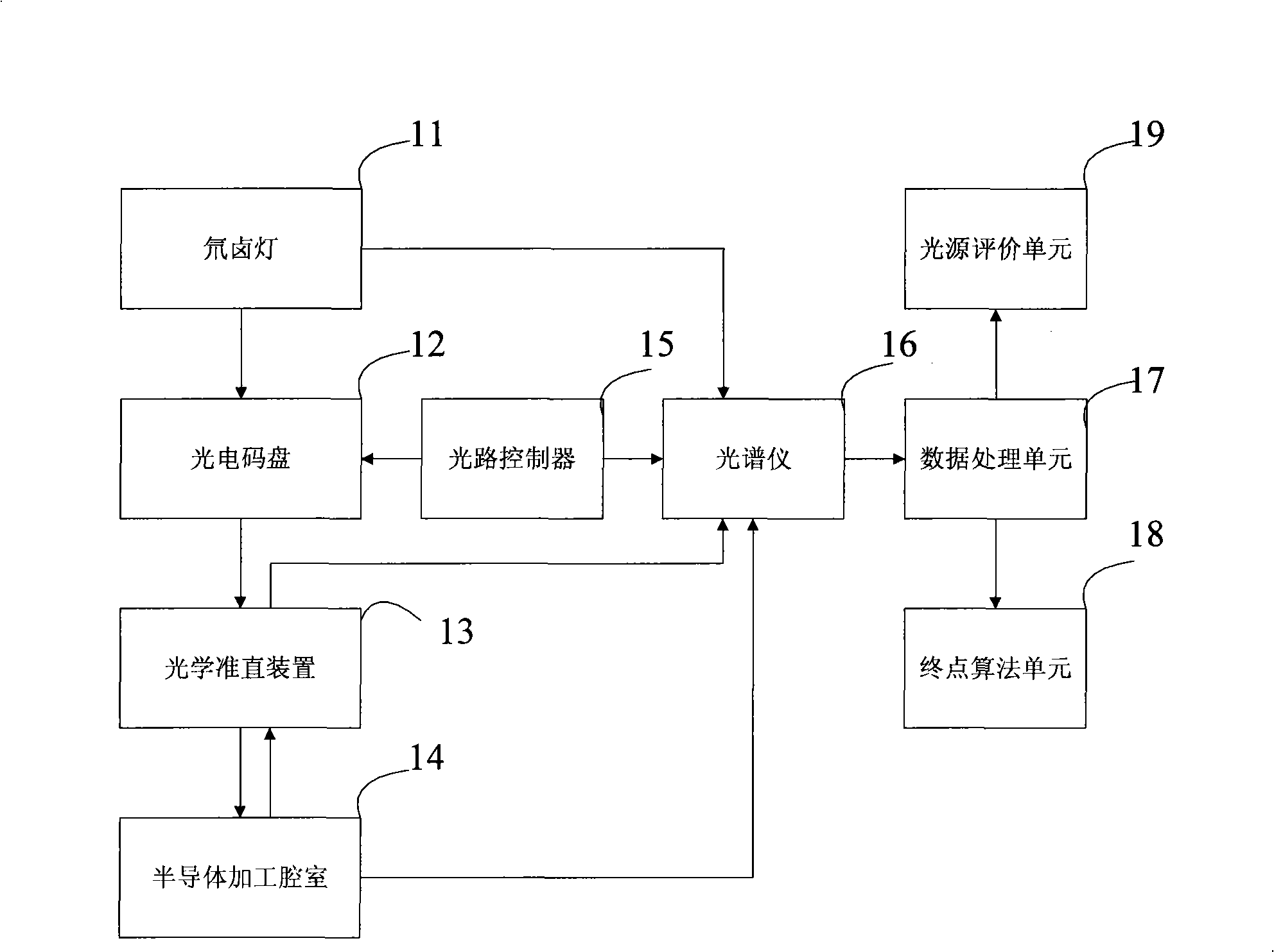
[0048] In the process of semiconductor processing process monitoring, the drift and disturbance of the intensity of the light source will reduce the resolution of the interference spectrum signal, which directly affects the accuracy and reliability of process monitoring. Therefore, the semiconductor processing process monitoring system and method described in this embodiment also A light source evaluation unit is provided to monitor the stability and lifetime of the continuous light source in real time. The following is attached image 3 and Figure 4 The present embodiment is explained.
[0049] Such as image 3 The monitoring system of the semiconductor processing technology described in the shown embodiment includes: a high-power deuterium-halogen lamp 11, a photoelectric code disc 12, an optical collimation device 13, an optical path controller 15, a multi-channel CCD spectrometer 16, and a data processing unit 17. An algorithm unit 18 and a light source evaluation unit...
Embodiment 3
[0054] Before the OES and IEP endpoint algorithms, it is necessary to perform data processing on the signals collected by the multi-channel CCD spectrometer 16 . The emission spectrum data records the plasma state of the reactive gas and generated gas participating in the etching process during the processing process, and the information that the strength of the same spectrum changes with the amount of reactants or products during the etching process; interference The spectral data records the periodically changing reflected light intensity information due to the change of the wafer film layer in the processing chamber during the process; and the light source intensity data records the change information of the light source intensity during the process.
[0055] This embodiment describes the processing method of the OES, IEP and light source intensity data of the semiconductor processing process monitoring system with reference to the accompanying drawings.
[0056] Such as ...
PUM
 Abstract
Description
Claims
Application Information
 - R&D Engineer
- R&D Manager
- IP Professional
- Industry Leading Data Capabilities
- Powerful AI technology
- Patent DNA Extraction
Browse by: Latest US Patents, China's latest patents, Technical Efficacy Thesaurus, Application Domain, Technology Topic, Popular Technical Reports.
© 2024 PatSnap. All rights reserved.Legal|Privacy policy|Modern Slavery Act Transparency Statement|Sitemap|About US| Contact US: help@patsnap.com