Method for activating magnesium doping gallium nitride base material and LED P-type gallium nitride

A gallium nitride-based, nitrogen-based technology, which is applied in the manufacture of semiconductor devices, electrical components, semiconductor/solid-state devices, etc., can solve the problems of GaN damage and failure, and achieve the effect of reducing negative effects and improving doping efficiency

Inactive Publication Date: 2009-07-01
PEKING UNIV
View PDF0 Cites 17 Cited by
  • Summary
  • Abstract
  • Description
  • Claims
  • Application Information

AI Technical Summary

Problems solved by technology

Oxygen plasma treated GaN has not received enough attention because it often exhibits damage characteristics

Method used


Image

  • Method for activating magnesium doping gallium nitride base material and LED P-type gallium nitride
  • Method for activating magnesium doping gallium nitride base material and LED P-type gallium nitride
  • Method for activating magnesium doping gallium nitride base material and LED P-type gallium nitride

Examples


Embodiment Construction

[0028] Below in conjunction with accompanying drawing and specific embodiment the present invention is described in further detail:

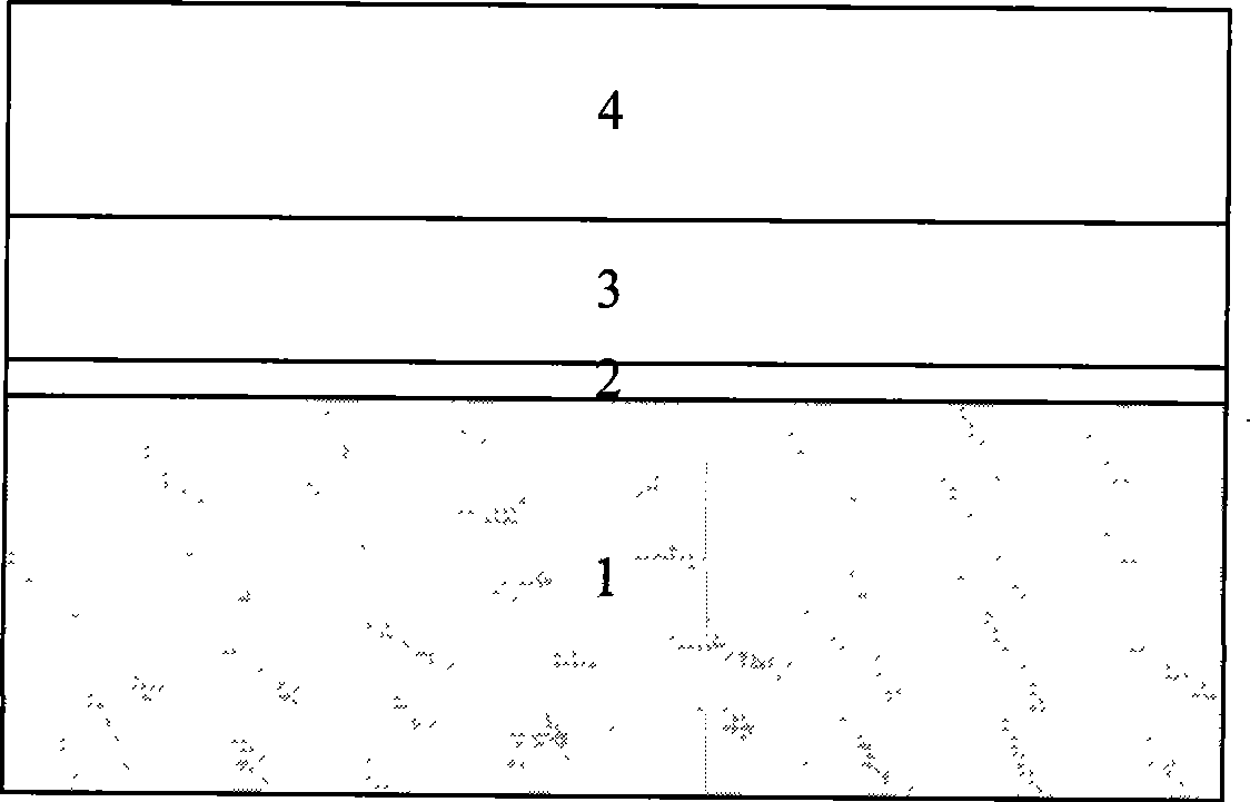
[0029] Such as figure 1 As shown, the single-layer Mg-doped GaN-based materials are from bottom to top: sapphire substrate 1, buffer layer 2, non-doped GaN (thickness more than 1 micron) 3, GaN:Mg (thickness greater than 300 nanometers) 4 .

[0030] refer to figure 2 , the above-mentioned Mg-doped GaN-based material is specifically processed as follows:

[0031] 1) Cleaning treatment of Mg-doped GaN-based material samples. First, the oxide layer and contamination on the surface of the sapphire substrate 1 and GaN:Mg4 are removed with a reducing liquid, and then the surface oil is further removed with an organic solvent, and then the GaN-based material sample is washed with deionized water.

[0032] 2) ICP processing. The reaction atmosphere is oxygen, the source power of the ICP can be adjusted between 100-500W, the bias power is 50-200W, t...


PUM


Abstract

The invention discloses an activation method of magnesium-doped nitride-based materials and luminescent diode P type gallium nitride, which comprises using an ICP plasma to process magnesium-doped nitride-based materials or luminescent diode P type gallium nitride, wherein reaction atmosphere comprises gas which contains oxygen element and mixed gas which contains oxygen element gas, or mixed gas of above gas with nitrogen, helium or argon gas, wherein the density of the plasma is between 1011-3 and 1012cm-3, then, removing oxidizing substance generated through the above reaction, and doing 400-600 EDG C high-temperature annealing to the materials. The activation method gets high-cavity density of magnesium-doped GaN materials, and improves the activation efficiency of magnesium-doped p-GaN.

Description

technical field [0001] The invention relates to a doping treatment method for GaN-based materials in the field of photoelectric technology, in particular to an activation method for magnesium-doped gallium nitride-based materials and light-emitting diode P-type gallium nitride. Background technique [0002] Mg is the main dopant that forms the P-type GaN material. In 1988, I.Akasaki and others in Japan obtained Mg-doped P-type GaN by means of low-energy electron irradiation (references I.Akasaki, T.Kozowa, K.Hiramatsu, N.Sawak, K.Ikeda, and Y.Ishi , Lumin., 40-41, 121(1988)), in 1992, S.Nakamura of Japan went a step further, he put Mg-doped GaN at 750℃ 2 Or vacuum annealing, also obtained p-type GaN (reference S.Nakamura, N.Iwasa, M.Senoh, and T.Mukai, Jpn.J.Appl.Phys, 34, L797 (1992)). Because of the acquisition of p-type GaN materials, the field of GaN-based devices has developed rapidly, and the semiconductor lighting revolution based on GaN-based light-emitting diodes ...

Claims


Application Information

Patent Timeline
Patent Type & Authority Applications(China)
IPC IPC(8): H01L33/00H01L21/30H01L21/324
Inventor 陈志忠齐胜利于彤军秦志新张国义
Owner PEKING UNIV
Why Eureka
Try Eureka