


Quick Research
Generate reliable direction feasibility study reports for your R&D in just a few steps.

Technical Q&A
Discover and master advanced knowledge NOW. Basics, ideas, possibilities, all at once.

Find Solutions
As an expert in R&D theories, this can generate solutions to your technical problems instantly.

Evaluate Feasibility
Analyze your overall solution with one click, know your potential R&D risks in advance.

Monitor Landscape
Get weekly tech updates, stay abreast of the latest tech innovations and key insights.
Solder ball loading method and solder ball loading apparatus
A technology of solder balls and pads, used in tin feeding devices, soldering equipment, assembling printed circuits with electrical components, etc., can solve problems such as solder bump peeling, and achieve high uniformity and good wettability.
- Summary
- Abstract
- Description
- Claims
- Application Information
AI Technical Summary
Problems solved by technology
Method used
Image

Examples
Embodiment 1
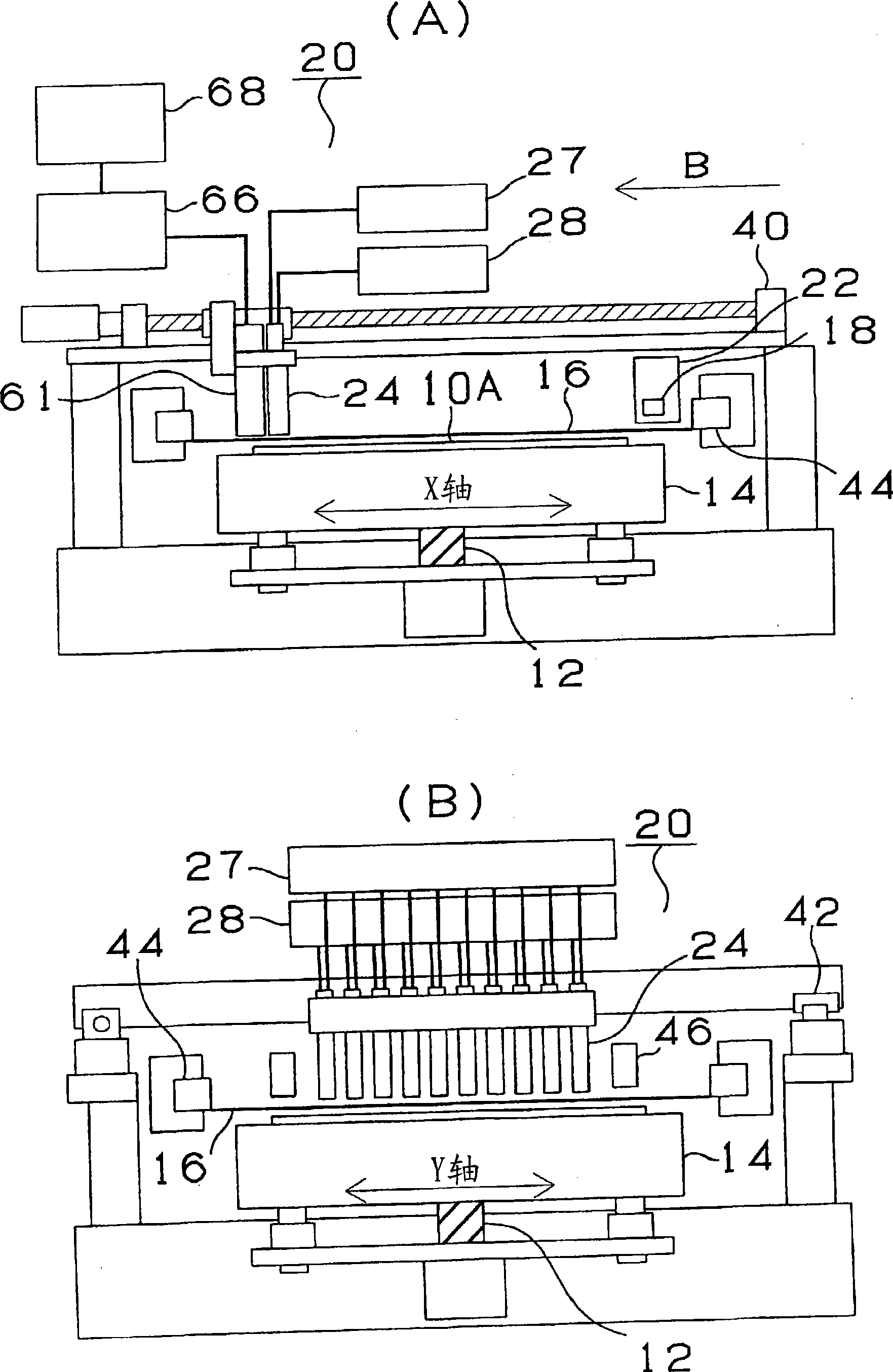
[0043] The solder ball loading device 20 of the first embodiment can transport solder balls by fixing the loading cylinder 24 and moving the ball array mask 16 and the printed wiring board 10 . In addition, the solder balls may be conveyed by moving the mounting cylinder 24 by fixing the ball array mask 16 and the printed wiring board 10 .
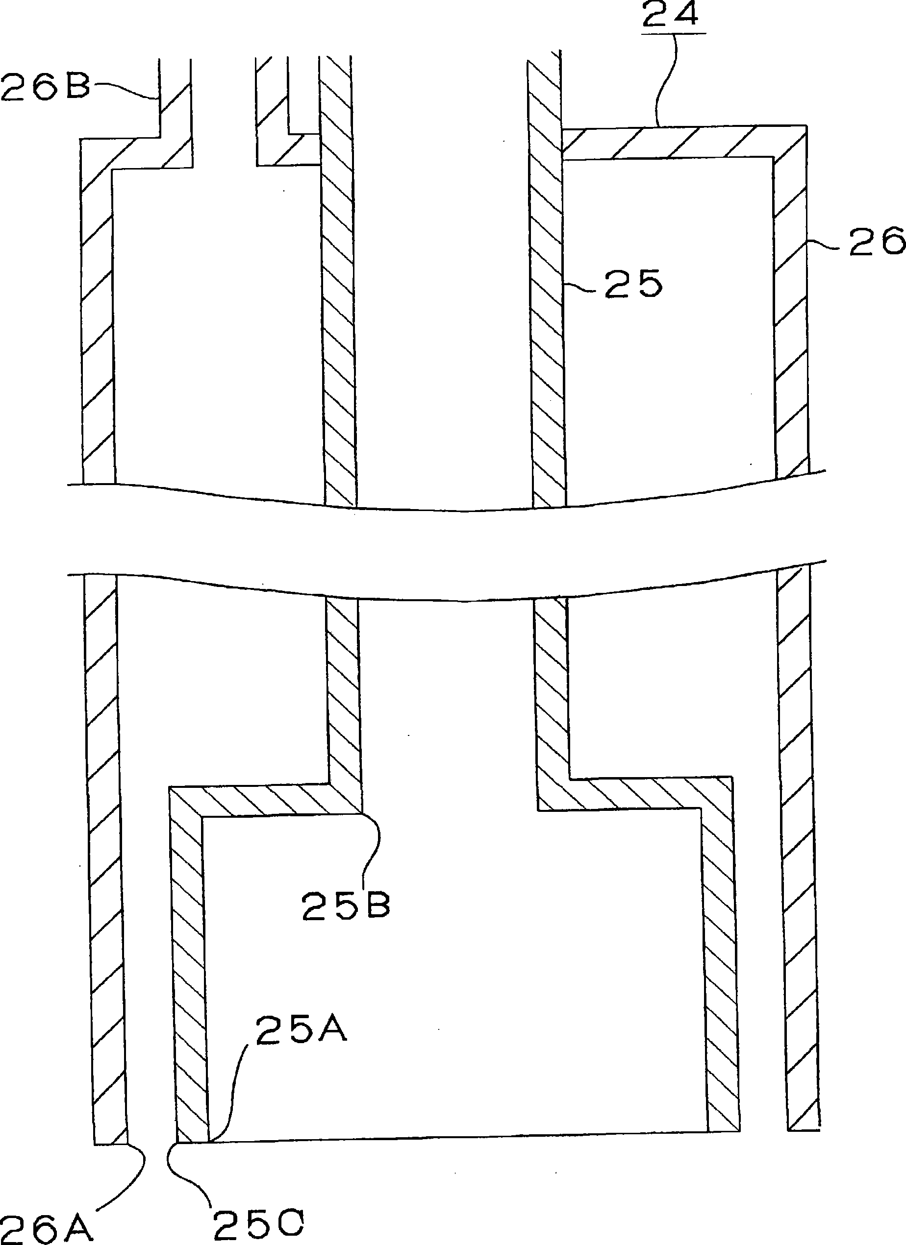
[0044] Refer to the section showing the cross section of the carrying cylinder 24 figure 2 The structure of the carrying cylinder 24 will be described.
[0045] The mounting cylinder 24 is composed of a supply cylinder 26 for supplying the inert gas and a suction cylinder 25 for sucking the supplied inert gas. figure 1 The inert gas supplied from the shown inert gas cylinder 28 through the pipe 26B is discharged from between the opening 26A of the supply cylinder 26 and the lower end periphery 25C of the suction cylinder 25 . On the other hand, using the figure 1 The negative pressure generated by the shown suction box 27 sucks the ine...
Embodiment 2
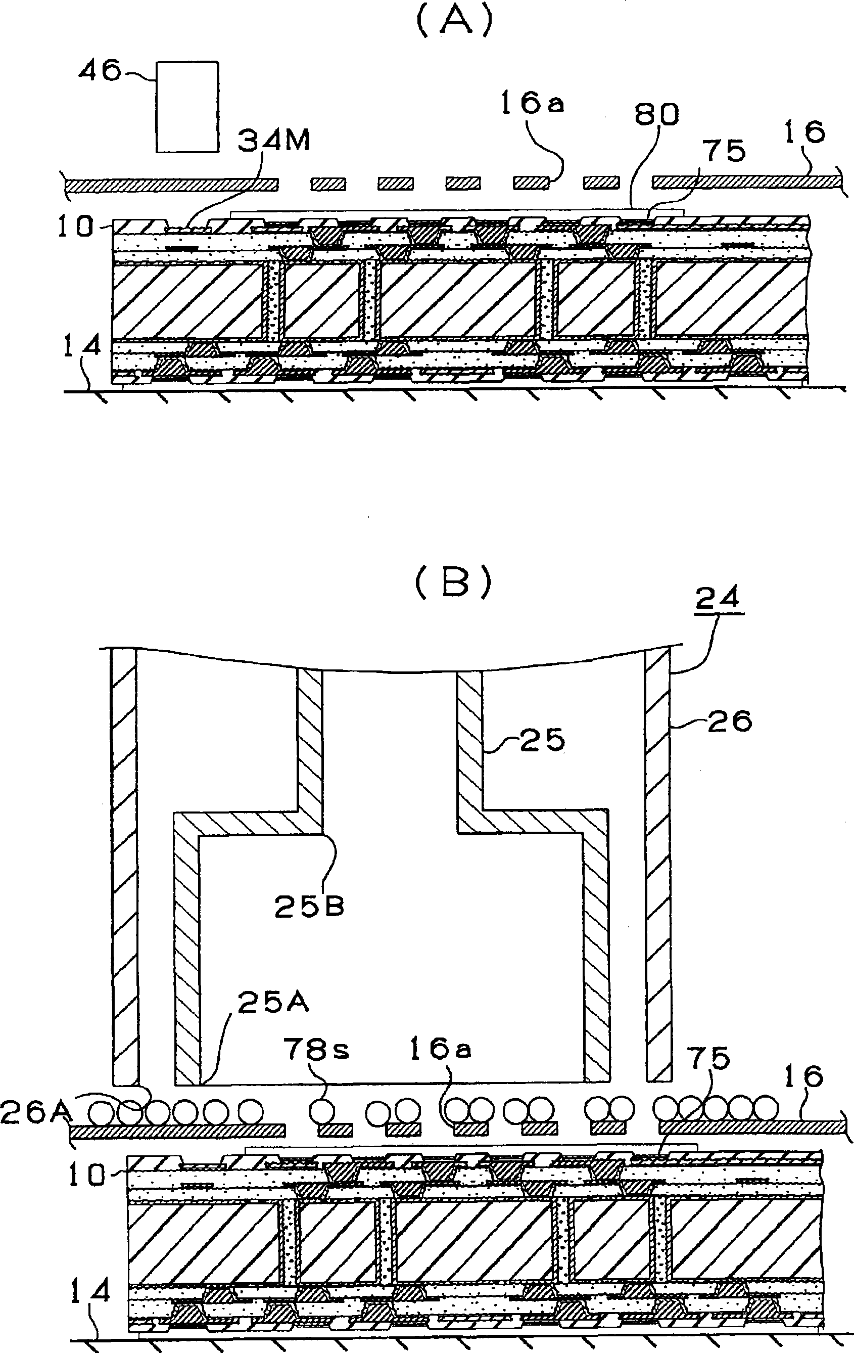
[0064] Figure 9 The mounting cylinder 125 of Example 2 is shown. refer to figure 2 , the above-mentioned carrying cylinder has a double structure, and the inert gas is supplied from the supply cylinder 26 outside the suction cylinder 25 . On the other hand, in Example 2, the nozzle 126 for supplying the inert gas is provided around the opening 125A of the mounting cylinder 125 . Even if the structure of this Example 2 is used, it is possible to prevent voids from being entangled in the solder bump in the same manner as in Example 1. FIG.
[0065] Next, the results of a comparison test between solder bumps manufactured by the solder ball mounting method of Example 1 and solder bumps manufactured by sucking air to transport the solder balls will be described.
[0066] Example 1
[0067] (1) Production of printed circuit boards
[0068]A double-sided copper-clad laminate (for example, MCL-E-67 manufactured by Hitachi Chemical Industries, Ltd.) is used as a material, and ...
PUM
| Property | Measurement | Unit |
|---|---|---|
| diameter | aaaaa | aaaaa |
| diameter | aaaaa | aaaaa |
| diameter | aaaaa | aaaaa |
Abstract
Description
Claims
Application Information
 - R&D Engineer
- R&D Manager
- IP Professional
- Industry Leading Data Capabilities
- Powerful AI technology
- Patent DNA Extraction
Browse by: Latest US Patents, China's latest patents, Technical Efficacy Thesaurus, Application Domain, Technology Topic, Popular Technical Reports.
© 2024 PatSnap. All rights reserved.Legal|Privacy policy|Modern Slavery Act Transparency Statement|Sitemap|About US| Contact US: help@patsnap.com