Manufacturing method for integrated schottky diode

A technology of Schottky diodes and manufacturing methods, which is applied in semiconductor/solid-state device manufacturing, electrical components, circuits, etc., and can solve the problem of uneven protection ring of integrated Schottky tubes, low and uniform breakdown voltage of integrated Schottky tubes Poor performance and other problems, to achieve the effect of uniform protection ring, easy repair interface layer, high breakdown voltage

Active Publication Date: 2010-08-11
SHANGHAI HUAHONG GRACE SEMICON MFG CORP
View PDF0 Cites 0 Cited by
  • Summary
  • Abstract
  • Description
  • Claims
  • Application Information

AI Technical Summary

Problems solved by technology

[0010] The Schottky diode produced by this method is shown in Figure 2. The oxide layer above the guard ring of the Schottky diode is an atmospheric pressure chemical vapor deposition oxide film (screen oxide APM), because the atmospheric pressure chemical vapor deposition oxide film (screen oxide APM) silicon wafers have poor in-plane uniformity, which will lead to uneven protection rings of integrated Schottky tubes formed during P-type source-drain injection. In addition, the film quality of the normal-pressure chemical vapor deposition oxide film (screen oxide APM) on the surface of the silicide is poor. , will also cause the breakdown voltage of the integrated Schottky tube to be low

Method used


Image

  • Manufacturing method for integrated schottky diode
  • Manufacturing method for integrated schottky diode
  • Manufacturing method for integrated schottky diode

Examples


Embodiment Construction

[0034] An embodiment of the integrated Schottky diode manufacturing method of the present invention is shown in Figure 3, comprises the following steps:

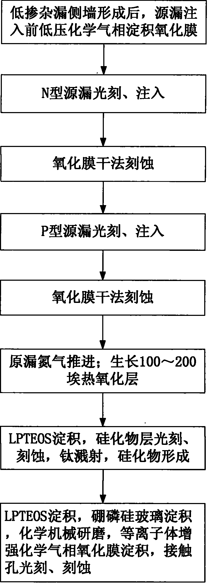
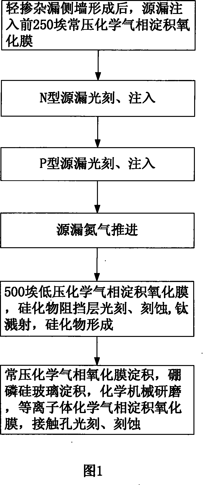
[0035] (1) Low-pressure chemical vapor deposition oxide film (LPTEOS) after the low-doped drain sidewall (LDD) is formed;

[0036] (2) N-type source-drain (NSD) lithography and implantation;

[0037] (3) LPTEOS dry etching;

[0038] (4) P-type source-drain (PSD) lithography and implantation;

[0039] (5) LPTEOS dry etching;

[0040] (6) Source-drain (SD) nitrogen propulsion; growth of 100-200 angstrom thermal oxide layer;

[0041] (7) 500 Angstrom LPTEOS deposition, silicide layer (SB) photolithography, etching, titanium sputtering, silicide (silicide) formation;

[0042] (8) LPTEOS deposition, borophosphosilicate glass deposition (BPSG), chemical mechanical polishing (CMP), plasma enhanced chemical vapor deposition oxide film (PETEOS) deposition, contact hole (CT) lithography and etching.

[0043] The difference betwee...


PUM


Abstract

The invention discloses a manufacturing method of an integrated Schottky diode. A lightly doped drain side wall is formed and subject to low-pressure chemical vapor deposition, dry etching of the oxide film dry etching is performed after photoetching and implantation of N type source / drain and P type source / drain; and a thin thermal oxide layer is grown at the later stage of propelling source / drain nitrogen. The method helps greatly improve the uniformity of breakdown voltage of the Schottky diode without changing the existing process sequence and adding a heating process.

Description

technical field [0001] The invention belongs to the field of semiconductor manufacturing, relates to a semiconductor device manufacturing process, in particular to a method for manufacturing an integrated Schottky diode. Background technique [0002] Schottky diodes are often integrated in IC integration processes because of their on-state voltage drop, high current, low power consumption, and extremely short reverse recovery time. For example, use its on-state voltage drop characteristics to clamp the bipolar transistor to prevent it from entering the deep saturation region to improve the frequency response of the circuit, or use its on-state voltage drop, high current, and low power consumption characteristics for output rectification to improve The drive capability of the circuit. However, due to the complex process of the integrated Schottky diode, there are many factors affected, so it is very difficult to make the electrical parameters uniform in the silicon wafer. ...

Claims


Application Information

Patent Timeline
Patent Type & Authority Patents(China)
IPC IPC(8): H01L21/82
Inventor 马清杰康志潇金勤海
Owner SHANGHAI HUAHONG GRACE SEMICON MFG CORP
Why Eureka
Try Eureka