Solid electrolyte silver germanium oxygen thin film and preparation method and use thereof
A solid electrolyte and thin film technology, applied in the field of microelectronic materials, can solve problems such as complex structure, writing and reading rely on mechanical movement, and difficult to further increase recording density
- Summary
- Abstract
- Description
- Claims
- Application Information
AI Technical Summary
Problems solved by technology
Method used
Image
Examples
Embodiment 1
[0047] The preparation method of the solid electrolyte film Ag-Ge-O, the preparation steps are as follows:
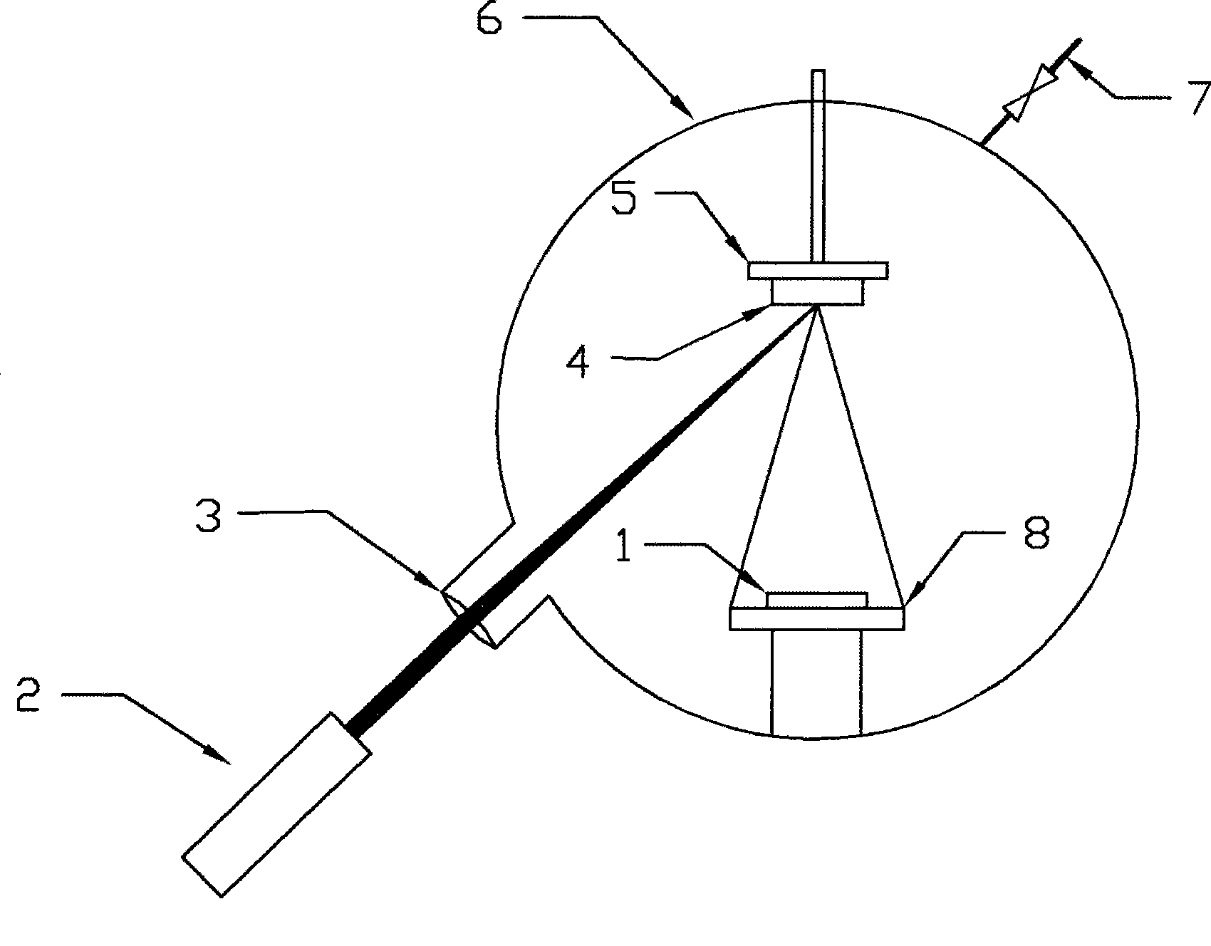
[0048] a) Ag-Ge-O ceramic target 4 is made of Ag 2 O, GeO 2 Powder mixed solid phase sintering preparation; Ag 2 O, GeO 2 The powders are uniformly mixed at a molar ratio of 1:1, ball milled for 12 hours, then sintered at 600°C, and cooled to make Ag-Ge-O ceramic target 4;
[0049] b) Fix the Ag-Ge-O ceramic target 4 in the pulsed laser deposition film forming system (e.g. figure 1 (Shown) on the target stage 5, the substrate 1 is fixed on the substrate stage 8, and they are all placed in the growth chamber 6 of the pulsed laser deposition film forming system;
[0050] c) Use a vacuum pump to vacuum the growth chamber 6 to 1.0×10 through the interface valve 7 of the mechanical pump and the molecular pump -3 Pa below;
[0051] d) Use KrF excimer laser 2, wavelength 248nm, pulse width 30ns, single pulse energy 300mJ, energy density 2.0J / cm 2 , Start the laser, make the laser...
Embodiment 2
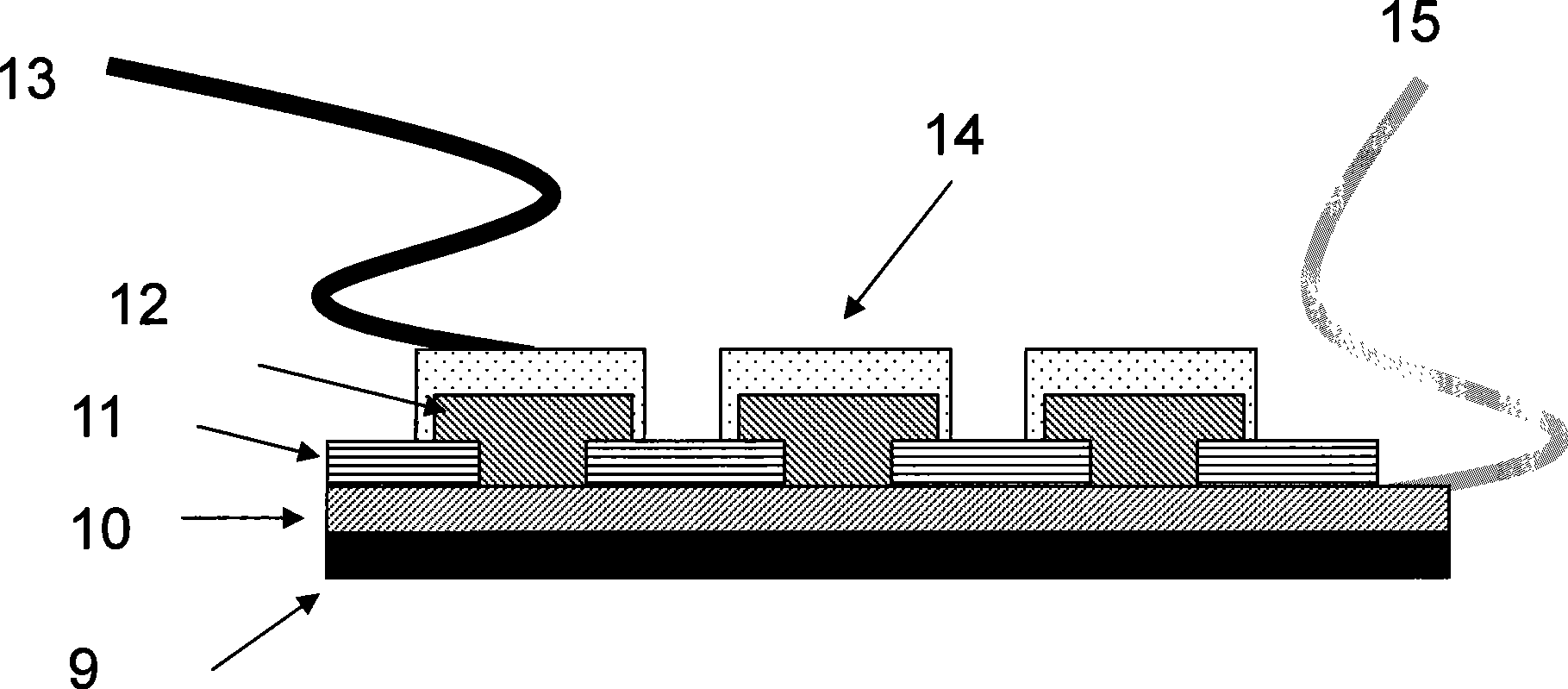
[0054] The preparation method of the non-volatile phase change memory element using the solid electrolyte film Ag-Ge-O, the specific preparation steps are as follows:
[0055] 1) The non-reactive electrode film 10 is deposited on the silicon wafer substrate 9 by a DC magnetron sputtering method, the material of which is platinum, and the thickness of the non-reactive electrode film 10 is 1 micron;
[0056] 2) Depositing an insulating layer 11 on the non-reactive electrode film 10 by using a radio frequency magnetron sputtering method, the material of the insulating layer is silicon dioxide, and its thickness is 120 nanometers;
[0057] 3) Cover the substrate with a metal mask engraved with a hole of 0.2mm in diameter, and process a micro hole with a diameter of 300 nanometers in the insulating layer 11 by focused ion beam etching, exposing the lower non-reactive electrode film 10;
[0058] 4) Put the substrate covered with the mask into the pulsed laser deposition chamber, and use...
PUM
| Property | Measurement | Unit |
|---|---|---|
| wavelength | aaaaa | aaaaa |
| energy | aaaaa | aaaaa |
| thickness | aaaaa | aaaaa |
Abstract
Description
Claims
Application Information
 - R&D Engineer
- R&D Manager
- IP Professional
- Industry Leading Data Capabilities
- Powerful AI technology
- Patent DNA Extraction
Browse by: Latest US Patents, China's latest patents, Technical Efficacy Thesaurus, Application Domain, Technology Topic, Popular Technical Reports.
© 2024 PatSnap. All rights reserved.Legal|Privacy policy|Modern Slavery Act Transparency Statement|Sitemap|About US| Contact US: help@patsnap.com


