Method for preparing nano CMOS integrated circuit by SiO2 masking technique
An integrated circuit, nano-scale technology, applied in circuits, electrical components, semiconductor/solid-state device manufacturing, etc., can solve problems such as waste of resources and energy, restrict the development of the semiconductor industry, etc., achieve a small conductive channel, achieve leapfrog development, Achieving processing-level effects
- Summary
- Abstract
- Description
- Claims
- Application Information
AI Technical Summary
Problems solved by technology
Method used
Image

Examples
Embodiment 1
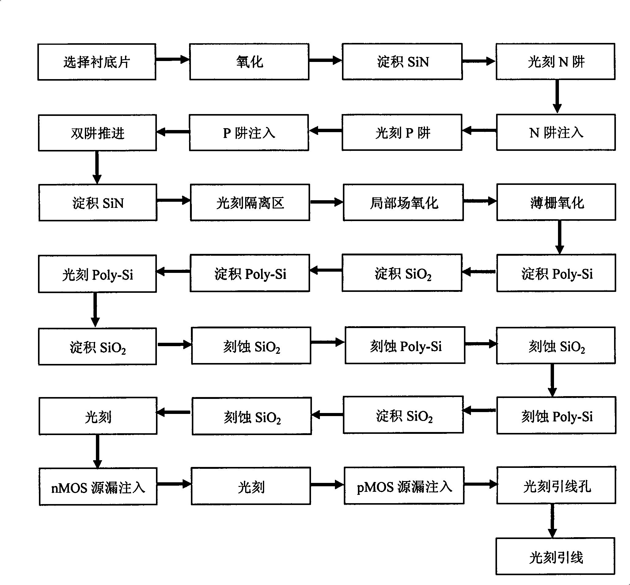
[0030] Embodiment 1: prepare the CMOS integrated circuit that conduction channel is 75nm on Si substrate, concrete steps are as follows:
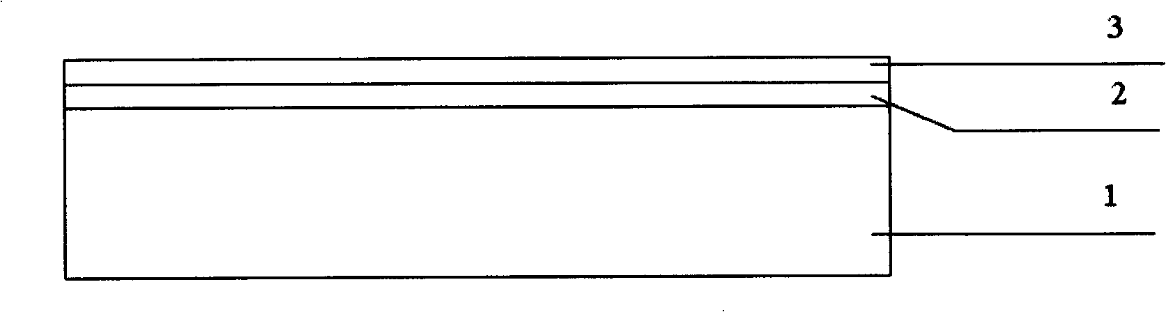
[0031] Step 1, depositing a masking layer, as shown in Figure 2(a).
[0032] (1a) Select the crystal orientation as and the doping concentration as 10 15 cm -3 Left and right p-type Si substrate sheets 1;
[0033] (1b) Thermally oxidize a layer of SiO with a thickness of 40 nm on the substrate 2 buffer layer 2;
[0034] (1c) on SiO 2 A 100nm thick SiN layer 3 is deposited on the buffer layer by plasma-enhanced chemical vapor deposition (PECVD) for masking implantation in the well region.
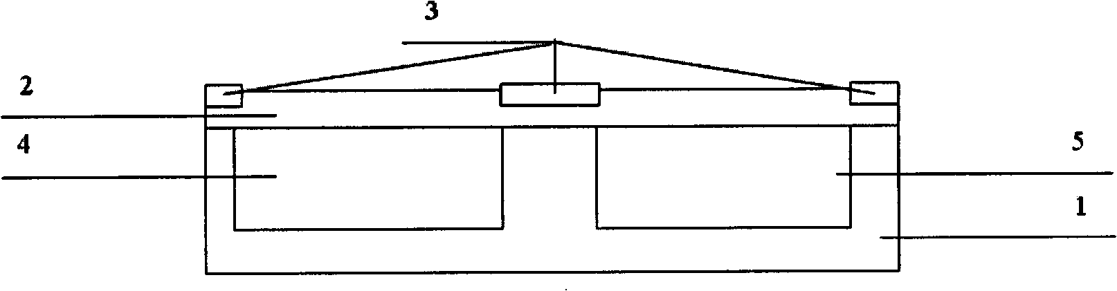
[0035] Step 2, forming a well region, as shown in FIG. 2(b).
[0036] (2a) Photoetching the P well region 4 and the N well region 5 on the SiN layer 3 according to the phase sequence;
[0037] (2b) Boron is implanted in the P well region to form a p-type region, and SiO is thermally oxidized on the surface of the P well region 2 , while advancing...
Embodiment 2
[0065] Embodiment 2: prepare the CMOS integrated circuit that conduction channel is 65nm on SOI substrate, concrete steps are as follows:
[0066] Step 1, depositing a masking layer, as shown in Figure 2(a).
[0067] (1a) Select the crystal orientation as and the doping concentration as 10 15 cm -3 left and right p-type SOI substrates 1;
[0068] (1b) Thermally oxidize a layer of SiO with a thickness of 40 nm on the substrate 2 buffer layer 2;
[0069] (1c) on SiO 2 A 150nm-thick SiN layer 3 is deposited on the buffer layer by means of atmospheric pressure chemical vapor deposition APCVD, which is used for the masking of well region implantation.
[0070] Step 2, forming a well region, as shown in FIG. 2(b).
[0071] (2a) Photoetching the P well region 4 and the N well region 5 on the SiN layer 3 according to the phase sequence;
[0072] (2b) Boron is implanted in the P well region to form a p-type region, and SiO is thermally oxidized on the surface of the P well regi...
Embodiment 3
[0100] Embodiment 3: prepare the CMOS integrated circuit that conduction channel is 90nm on Si substrate, concrete steps are as follows:
[0101] Step 1, depositing a masking layer, as shown in Figure 2(a).
[0102] (1a) Select the crystal orientation as and the doping concentration as 10 15 cm -3 Left and right p-type Si substrate sheets 1;
[0103] (1b) Thermally oxidize a layer of SiO with a thickness of 60 nm on the substrate 2 buffer layer 2;
[0104] (1c) on SiO 2 A 200nm-thick SiN layer 3 is deposited on the buffer layer by low-pressure chemical vapor deposition (LPCVD) for masking of well implantation.
[0105] Step 2, forming a well region, as shown in FIG. 2(b).
[0106] (2a) Photoetching the P well region 4 and the N well region 5 on the SiN layer 3 according to the phase sequence;
[0107] (2b) Boron is implanted in the P well region to form a p-type region, and SiO is thermally oxidized on the surface of the P well region 2 , while advancing the P well, f...
PUM
 Abstract
Description
Claims
Application Information
 - R&D
- Intellectual Property
- Life Sciences
- Materials
- Tech Scout
- Unparalleled Data Quality
- Higher Quality Content
- 60% Fewer Hallucinations
Browse by: Latest US Patents, China's latest patents, Technical Efficacy Thesaurus, Application Domain, Technology Topic, Popular Technical Reports.
© 2025 PatSnap. All rights reserved.Legal|Privacy policy|Modern Slavery Act Transparency Statement|Sitemap|About US| Contact US: help@patsnap.com