
Soldering method and semiconductor module manufacturing method

A welding method and technology of manufacturing method, applied in semiconductor/solid-state device manufacturing, semiconductor device, welding equipment and other directions, can solve the problems of increasing welding man-hours and complex structure, etc.

Inactive Publication Date: 2009-01-21
TOYOTA IND CORP
View PDF4 Cites 4 Cited by
  • Summary
  • Abstract
  • Description
  • Claims
  • Application Information

AI Technical Summary

Problems solved by technology

However, in a semiconductor module constructed by soldering a plurality of semiconductor elements to a circuit board, if a guide is provided for each of the compacts placed on each of the plurality of semiconductor elements, the structure becomes complicated and the man-hours for soldering increase.

Method used


Image

  • Soldering method and semiconductor module manufacturing method
  • Soldering method and semiconductor module manufacturing method
  • Soldering method and semiconductor module manufacturing method

Examples

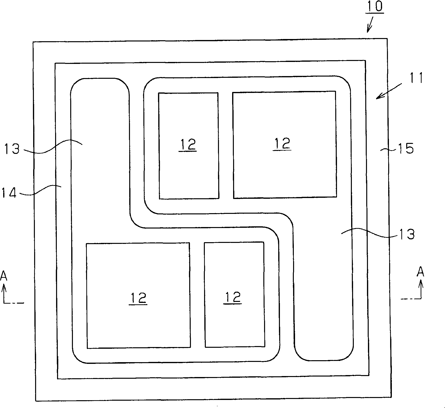
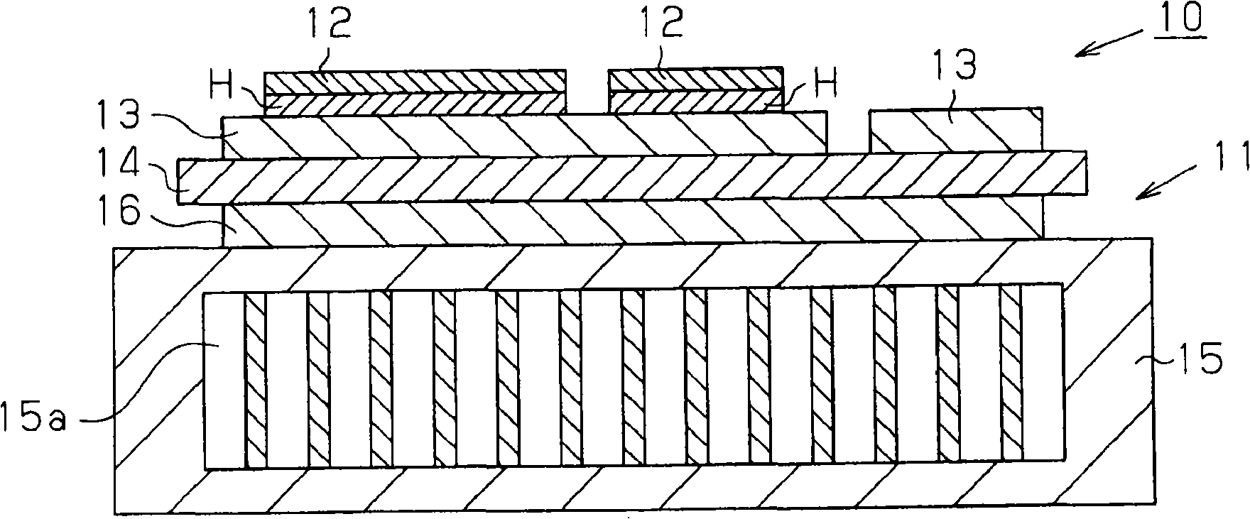

Embodiment Construction

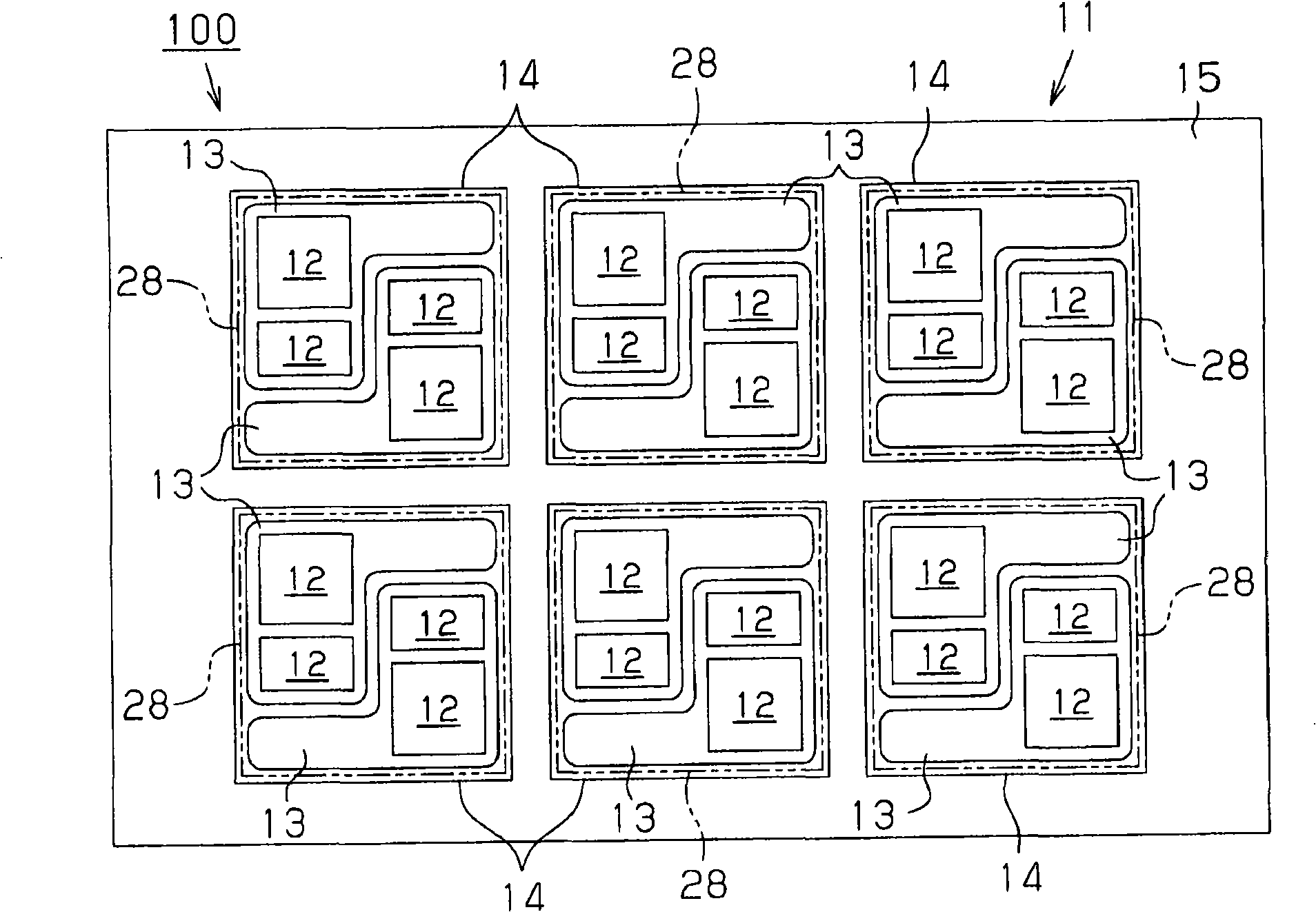
[0024] Below, according to figure 1 ˜ FIG. 5 describe a first embodiment that actualizes the present invention.

[0025] The semiconductor module 10 includes: a circuit board 11 ; and at least three semiconductor elements 12 that are not aligned on a straight line on the circuit board 11 . figure 1 and figure 2 The illustrated semiconductor module 10 includes four semiconductor elements 12 . The circuit board 11 includes: a ceramic substrate 14 as a ceramic insulator having a metal circuit 13 on its surface; and a metal heat sink 15 fixed to the ceramic substrate 14 via a metal plate 16 . That is, the circuit board 11 is a cooling circuit board, that is, a board with a heat sink. The radiator 15 is formed of aluminum-based metal, copper, or the like, and includes a refrigerant flow path 15 a through which a cooling medium flows. The aluminum-based metal refers to aluminum or an aluminum alloy. Metal plate 16 functions as a bonding layer for bonding ceramic substrate 14 a...


PUM


Abstract

Disclosed is a method for soldering semiconductor elements on bonding sections arranged at a plurality of areas on a circuit board, respectively. The soldering method is provided with a step of arranging the bonding sections in nonlinear arrangement on at least three areas on the circuit board; a step of arranging the semiconductor elements on the bonding sections through a solder; a step of placing a guard over the at least three semiconductor elements nonlinearly arranged; and a step of melting the solder while applying pressure to the semiconductor elements by the guard, and thus soldering the semiconductor elements on the bonding sections. As a result, at the time of soldering the semiconductor elements on the circuit board, fluctuation in solder thickness at the bonding sections is suppressed.

Description

technical field [0001] The present invention relates to a method of soldering a plurality of semiconductor elements on a circuit board and a method of manufacturing a semiconductor module. Background technique [0002] When mounting a semiconductor element or an electronic component on a circuit board, it is generally a method of joining the circuit board, the semiconductor element, and the like via solder. In the case of soldering a semiconductor element, etc. to a circuit board, when the solder interposed between the semiconductor element, etc. and the circuit board melts, the position of the semiconductor element, etc. The solder does not spread over the entire bonding surface of the semiconductor element or the like and is bonded. As a method of suppressing such inconveniences, for example, methods disclosed in Patent Documents 1, 2, 3, and 4 have been proposed. In Patent Documents 1 and 2, when soldering the semiconductor element on the substrate by reflowing the sold...

Claims


Application Information

Patent Timeline
Patent Type & Authority Applications(China)
IPC IPC(8): H01L21/52B23K1/00B23K3/00H01L25/07H01L25/18H05K3/34
CPCH01L2924/09701H01L24/95H05K3/0061H05K2203/0278H01L24/83H01L24/29H01L2224/32225H01L2924/0105H01L2924/1305H01L2224/97H05K2203/159H05K3/3494H05K2203/101H01L2924/01004H01L2924/01006H01L2924/13055H05K3/341H01L2224/83801B23K1/0016H01L2924/01005H01L2924/01082H01L2924/19042H01L2924/01013H05K1/0306H01L2224/29101H01L2924/014H01L2924/01023H01L2924/01029B23K2201/40H01L2924/01033H01L2924/15787B23K2101/40H01L2224/75266Y02P70/50H01L2224/83H01L2924/00
Inventor 金原雅彦
Owner TOYOTA IND CORP
Learn More