LED heating heat sink rear using laser and heat sink bonding method
A LED chip and heat sink technology, which is applied in the field of LED chip and heat sink bonding, can solve problems such as gasification, failure to ensure reliable bonding of LED chip and heat sink, and solder oxidation, so as to avoid oxidation and gasification, and facilitate The effect of automation and high production efficiency
- Summary
- Abstract
- Description
- Claims
- Application Information
AI Technical Summary
Problems solved by technology
Method used
Image
Examples
specific Embodiment approach 1
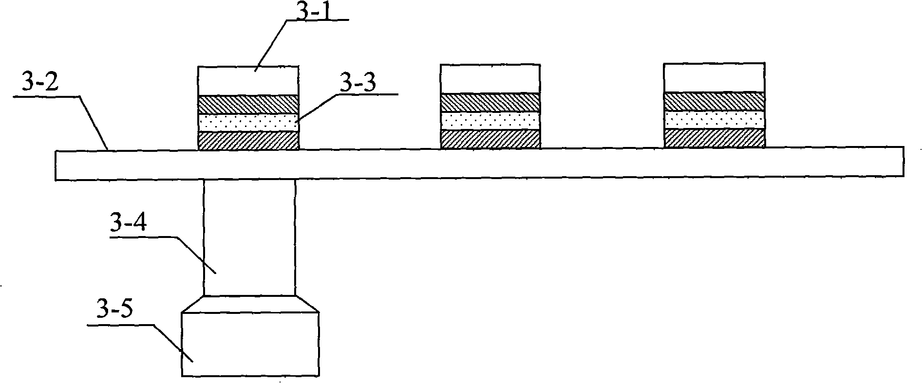
[0012] Specific implementation mode one: combine image 3 , to illustrate the LED chip and heat sink bonding method described in this embodiment using laser heating on the back of the heat sink. Its specific steps are:
[0013] Step 1. Plating Au on the back of the LED chip 3-1 and the pads of the heat sink 3-2 respectively;
[0014] Step 2, plating or printing a solder layer 3-3 on the gold-plated Au pad;
[0015] Step 3, paste the LED chip 3-1 on the solder layer 3-3 of the gold-plated Au pad;
[0016] Step 4: Use the laser beam 3-4 to align the backside of the gold-plated Au pad on the heat sink 3-2 and heat until the solder layer 3-3 melts.
[0017] The shape of the heat sink 3-2 in this embodiment is flat, U-shaped or fin-shaped.
[0018] The material of the heat sink 3-2 in this embodiment is copper Cu or aluminum Al.
[0019] The solder layer 3-3 in this embodiment mode is SnAg, SnAgCu, or PbSn.
[0020] In this embodiment, the laser beam 3-4 is used to locally hea...
specific Embodiment approach 2
[0021] Embodiment 2: In this embodiment, the bonding method described in Embodiment 1 is used to realize the bonding of multiple LED chips 3-1 and the heat sink 3-2. The specific process is as follows:
[0022] Repeat step 1 to achieve gold-plated Au on multiple pads on the back of multiple LED chips 3-1 and on the heat sink 3-2;
[0023] Repeat step 2 to plate or print solder layers 3-3 on multiple gold-plated Au pads;
[0024] Repeating step 3, attaching multiple LED chips 3-1 to the solder layers 3-3 of multiple gold-plated Au pads;
[0025] The heat sink 3-2 or the laser beam 3-4 is moved manually or automatically, and step 4 is repeated to realize the bonding of the LED chips 3-1 and the heat sink 3-2 one by one.
[0026] In this embodiment, the bonding of multiple LED chips 3 - 1 and the heat sink 3 - 2 is realized by repeating the steps described in the first embodiment.
[0027] The mounting of the brazing laser output lens 3-5 and the LED chip 3-1 in this embodiment...
specific Embodiment approach 3
[0028] Specific implementation mode three: combination Figure 5 , to describe this embodiment. The difference between the present embodiment and the specific embodiment 1 or 2 is that in the step 4, the laser spot pointer 3-7 is used to realize the alignment of the gold-plated Au pad with the laser beam 3-4.
[0029] The alignment method described in this embodiment is as follows: place the laser spot indicator 3-7 above the heat sink, fix the brazing laser output lens 3-5, and move the laser spot indicator 3-7 so that The laser indicating light 3-6 output by it coincides with the brazing laser beam 3-4 output by the brazing laser output lens 3-5, and the LED chip 3-1 to be bonded is positioned at the position by moving the heat sink 3-2. 3-6 times of the above-mentioned laser pointing light.
[0030] In this embodiment, a laser spot indicator 3-7 is added, which simplifies the alignment method between the laser beam 3-4 and the gold-plated Au pad, and facilitates automatic...
PUM
 Abstract
Description
Claims
Application Information
 - R&D
- Intellectual Property
- Life Sciences
- Materials
- Tech Scout
- Unparalleled Data Quality
- Higher Quality Content
- 60% Fewer Hallucinations
Browse by: Latest US Patents, China's latest patents, Technical Efficacy Thesaurus, Application Domain, Technology Topic, Popular Technical Reports.
© 2025 PatSnap. All rights reserved.Legal|Privacy policy|Modern Slavery Act Transparency Statement|Sitemap|About US| Contact US: help@patsnap.com


