Electric connecting structure of circuit board embedding with semiconductor chip
A semiconductor and circuit board technology, applied in semiconductor devices, semiconductor/solid-state device parts, circuits, etc., can solve problems such as thermal stress mismatch, inability to meet thin lines, separation of electrode pad surfaces, etc., to solve the problem of difficult matching of thermal expansion coefficients , to avoid the effect of separation of build-up lines and reduction of electrical quality
- Summary
- Abstract
- Description
- Claims
- Application Information
AI Technical Summary
Problems solved by technology
Method used
Image
Examples
no. 1 example
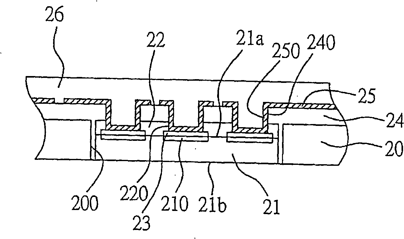
[0054] Such as figure 2 Shown is a schematic cross-sectional view of the first embodiment of the circuit board structure for embedding semiconductor chips of the present invention. As shown in the figure, the circuit board structure of the embedded semiconductor chip of the present invention includes: a support plate 20, at least one semiconductor chip 21, core surface protection layer 22, metal layer 23, dielectric layer 24, circuit layer 25 and hollow conductive Blind hole 250.
[0055] The support board 20 mentioned above can be a circuit board, an insulating board, or a core board, and the material of the core board can be metal or non-metal. In addition, at least one opening 200 is formed in the support plate 20 for accommodating the semiconductor chip 21 .
[0056] The semiconductor chip 21 has an active surface 21a and an opposite passive surface 21b, and a plurality of electrode pads 210 are formed on the active surface 21a.
[0057] The core protection layer 22 is...
no. 2 example
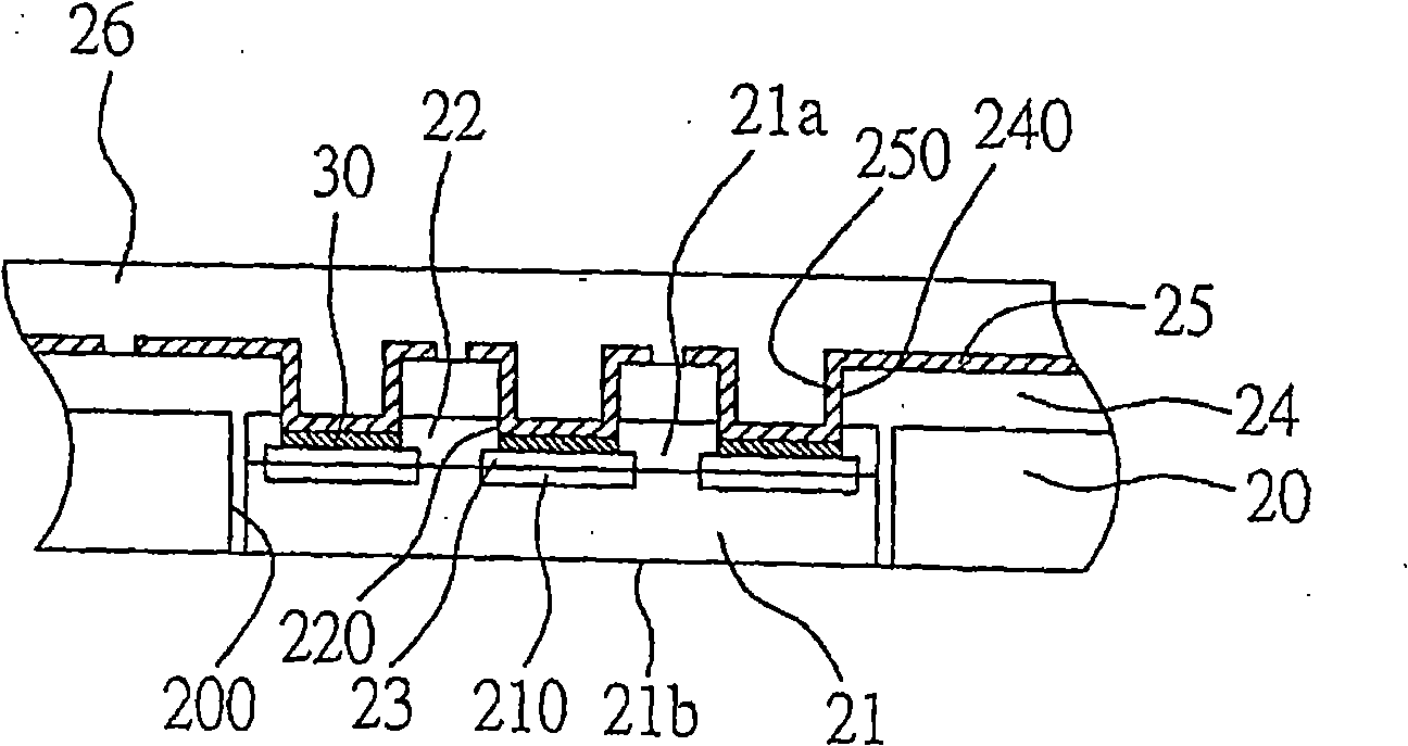
[0064] Such as image 3 Shown is a schematic cross-sectional view of the second embodiment of the circuit board structure for embedding semiconductor chips of the present invention.
[0065] The structure of the circuit board embedded with semiconductor chips in this embodiment is substantially the same as that of the first embodiment, the main difference is that this embodiment further includes a buffer metal layer.
[0066] Such as image 3 As shown, a buffer metal layer 30 is formed between the above-mentioned hollow conductive blind hole 250 and the metal layer 23, and the buffer metal layer 30 can be copper foil, so that when the thickness of the metal layer 23 is insufficient, the thickened The buffer metal layer 30 is used as a blocking layer for subsequent laser drilling of the dielectric layer 24 to form holes (ie, blind holes), thereby preventing the electrode pads 210 of the semiconductor chip 21 covered thereunder from being damaged.
no. 3 example
[0068] Such as Figure 4 Shown is a schematic cross-sectional view of a third embodiment of the circuit board structure for embedding semiconductor chips of the present invention.
[0069] In this embodiment, the structure of the circuit board for embedding semiconductor chips is roughly the same as that of the aforementioned first embodiment. The circuit build-up structure 40 on the surface of 25 .
[0070] The circuit build-up structure 40 includes at least one dielectric layer 400, a circuit layer 402 stacked on the surface of the dielectric layer 400, and a full circuit layer 402 formed in the dielectric layer 400 for electrically connecting the circuit layer 402 to the circuit layer 25. The metal-plated blind hole 404 ; of course, a hollow conductive blind hole (not shown) can also be used as a telecommunication conduction path between the circuit layer 402 and the circuit layer 25 .
[0071] The dielectric layer 400 fills the hollow conductive blind hole 250 . In this...
PUM
 Abstract
Description
Claims
Application Information
 - Generate Ideas
- Intellectual Property
- Life Sciences
- Materials
- Tech Scout
- Unparalleled Data Quality
- Higher Quality Content
- 60% Fewer Hallucinations
Browse by: Latest US Patents, China's latest patents, Technical Efficacy Thesaurus, Application Domain, Technology Topic, Popular Technical Reports.
© 2025 PatSnap. All rights reserved.Legal|Privacy policy|Modern Slavery Act Transparency Statement|Sitemap|About US| Contact US: help@patsnap.com


