A belt clearance width modulating gallium indium oxide film and its making method
A technology of oxide thin film and gallium indium, which is applied in the field of gallium indium oxide thin film materials and its preparation, can solve the problems of inability to modulate, excessive bandgap width, difficulties, etc., achieve good uniformity and repeatability, and facilitate the industry Chemical, good adhesion performance
- Summary
- Abstract
- Description
- Claims
- Application Information
AI Technical Summary
Benefits of technology
Problems solved by technology
Method used
Image
Examples
Embodiment 1
[0049] Embodiment 1: MOCVD technology prepares Ga 0.2 In 1.8 o 3 Gallium Indium Oxide Thin Film Material
[0050] (1) First pump the reaction chamber of the MOCVD equipment to a high vacuum state of 5×10 -4 Pa, heat the substrate to 550°C;
[0051] (2) Open the valve of the nitrogen cylinder and feed nitrogen into the reaction chamber (background N 2 )300sccm, 30 minutes, make reaction chamber pressure be 50Torr;
[0052] (3) Open the valve of the oxygen cylinder, adjust the flow rate of oxygen to 50 sccm, and keep it for 10 minutes;
[0053] (4) Open the valve of the indium source bottle, adjust the flow rate of the carrier gas (nitrogen) to 20 sccm, and keep it for 10 minutes;
[0054] (5) Open the valve of the gallium source bottle, adjust the flow of carrier gas (nitrogen) to 1 sccm, and keep it for 10 minutes;
[0055] (6) Pass oxygen and organometallic sources (gallium source and indium source) into the reaction chamber at the same time, and keep the film growth t...
Embodiment 2
[0059] Embodiment 2: MOCVD technology prepares Ga 0.4 In 1.6 o 3 Gallium Indium Oxide Thin Film Material
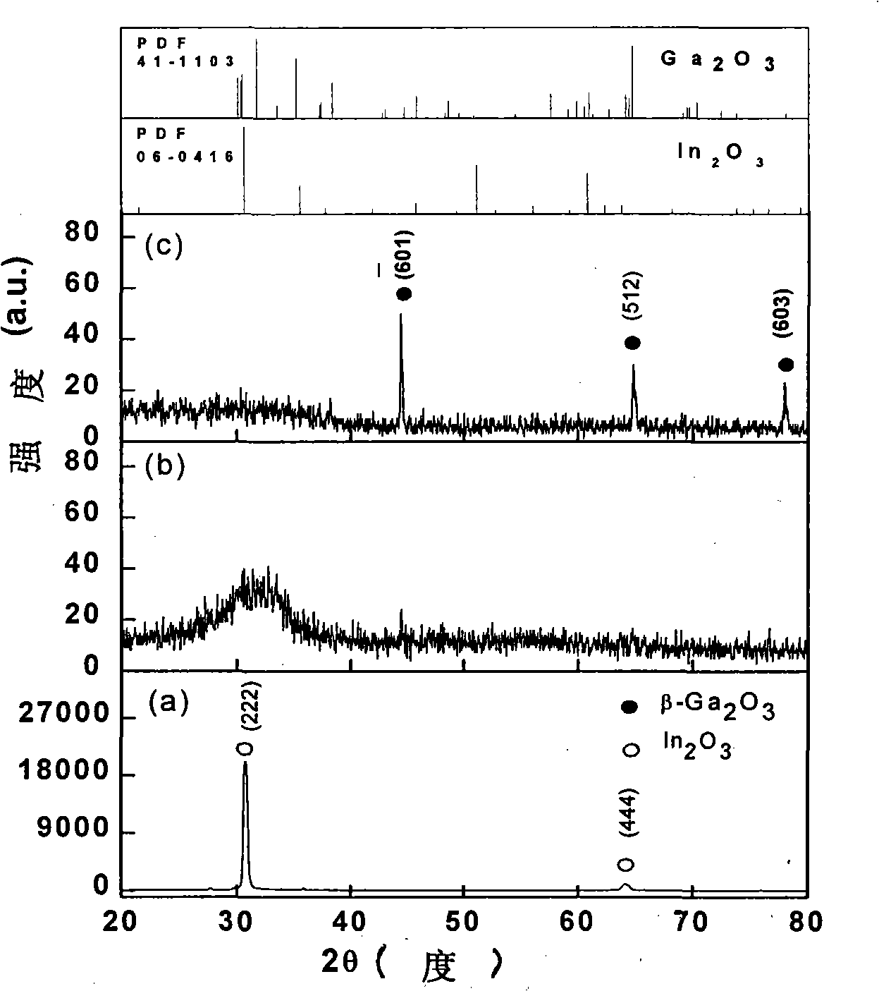
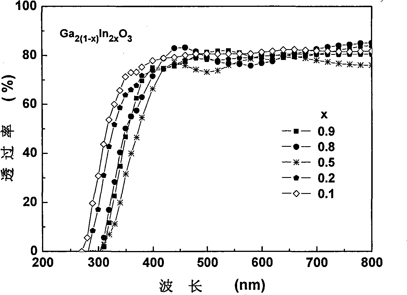
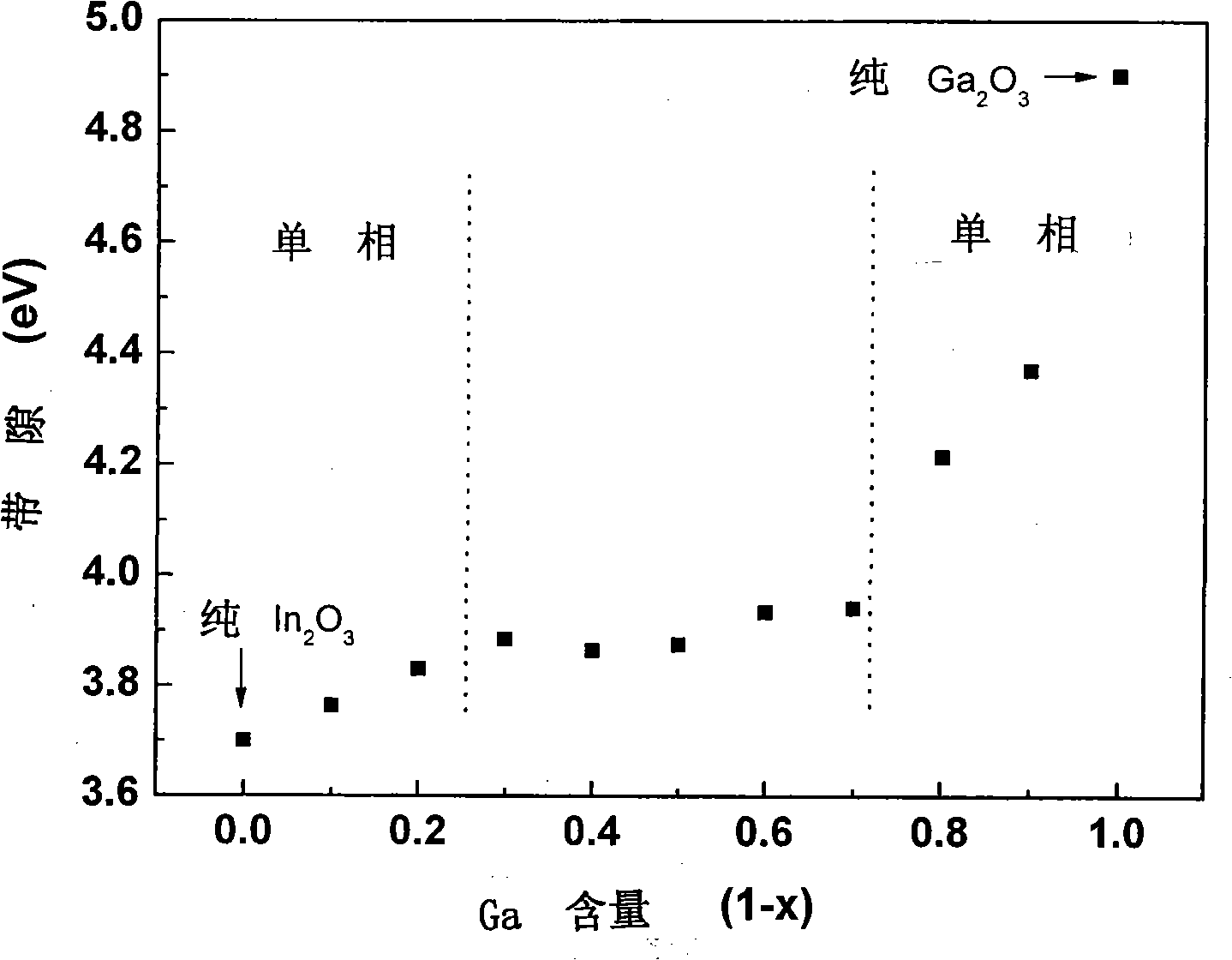
[0060] The gallium indium oxide thin film material was prepared by MOCVD technology. The preparation method and process conditions were the same as in Example 1, except that the organometallic gallium source temperature was -14°C, the organometallic indium source was 28°C, the growth temperature (substrate temperature) was 550°C, and the organometallic gallium source temperature was -14°C. The gallium source carrier gas flow rate is 2.6 sccm, the organic metal indium source carrier gas flow rate is 25 sccm, the growth time is 300 minutes, and the film thickness is 502 nm. The film is cubic In 2 o 3 Single crystal structure, the bandgap width of the film is 3.83eV, and the average relative transmittance in the visible light range exceeds 85%.
Embodiment 3
[0061] Embodiment 3: MOCVD technology prepares Ga 0.4 In 1.6 o 3 Gallium Indium Oxide Thin Film Material
[0062] The preparation method and process conditions are the same as those in Example 2, except that the growth temperature is 700° C., the growth time is 300 minutes, and the film thickness is 410 nm. The prepared film is cubic In 2 o 3 Single crystal structure, the bandgap width of the film is 3.78eV, and the average relative transmittance in the visible light range exceeds 83%.
PUM
| Property | Measurement | Unit |
|---|---|---|
| Band gap width | aaaaa | aaaaa |
| Thickness | aaaaa | aaaaa |
| Band gap width | aaaaa | aaaaa |
Abstract
Description
Claims
Application Information
 - R&D
- Intellectual Property
- Life Sciences
- Materials
- Tech Scout
- Unparalleled Data Quality
- Higher Quality Content
- 60% Fewer Hallucinations
Browse by: Latest US Patents, China's latest patents, Technical Efficacy Thesaurus, Application Domain, Technology Topic, Popular Technical Reports.
© 2025 PatSnap. All rights reserved.Legal|Privacy policy|Modern Slavery Act Transparency Statement|Sitemap|About US| Contact US: help@patsnap.com


