Semiconductor substrate surface chemical processing method apparatus

A technology for chemical treatment and substrate surface, which is applied in the field of wet chemical treatment of semiconductor substrates and chemical treatment of semiconductor substrates. It can solve problems such as failure to meet requirements, poor uniformity, increase the steps of coating and cleaning films, etc., to increase distance, The effect of increasing the distance and eliminating the possibility

Active Publication Date: 2008-09-03
WUXI SUNTECH POWER CO LTD
View PDF0 Cites 9 Cited by
  • Summary
  • Abstract
  • Description
  • Claims
  • Application Information

AI Technical Summary

Problems solved by technology

However, the above-mentioned method of protecting with a mask and then performing wet chemical treatment also has great disadvantages: it not only increases the steps of coating and cleaning the film in the operation process, but also increases the cost of raw materials and the amount of wastewater generated during the treatment process.
In the above two cases, chemical treatment will be performed on the upper surface of the semiconductor substrate that does not need to be processed, so that the quality of the semiconductor substrate is unqualified or the uniformity is very poor, which cannot meet the requirements

Method used


Image

  • Semiconductor substrate surface chemical processing method apparatus
  • Semiconductor substrate surface chemical processing method apparatus
  • Semiconductor substrate surface chemical processing method apparatus

Examples


specific Embodiment 1

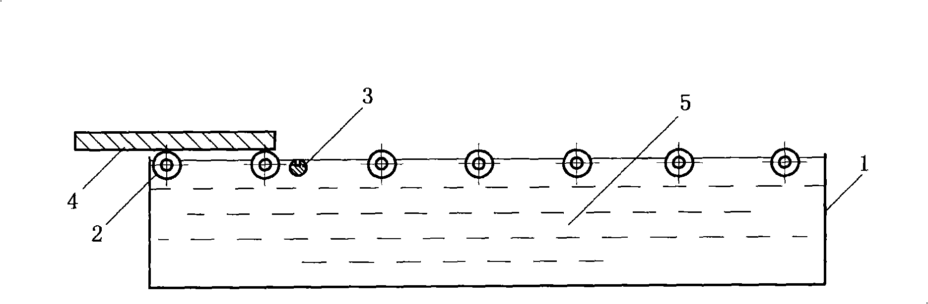
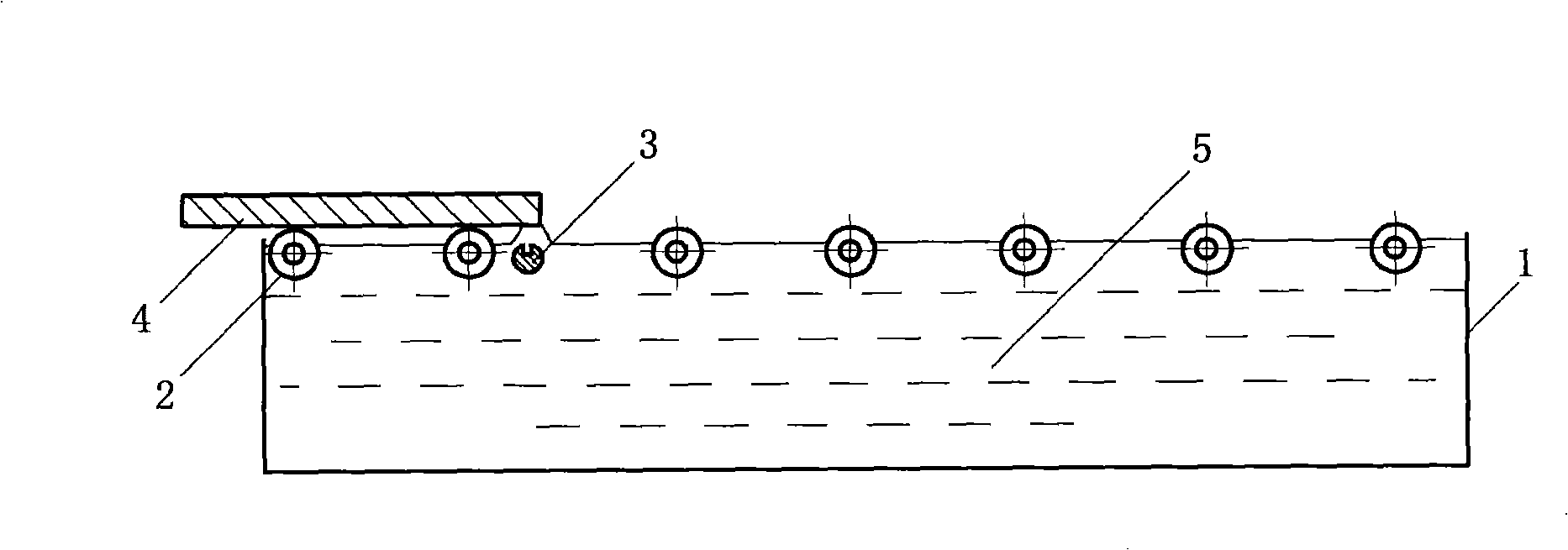
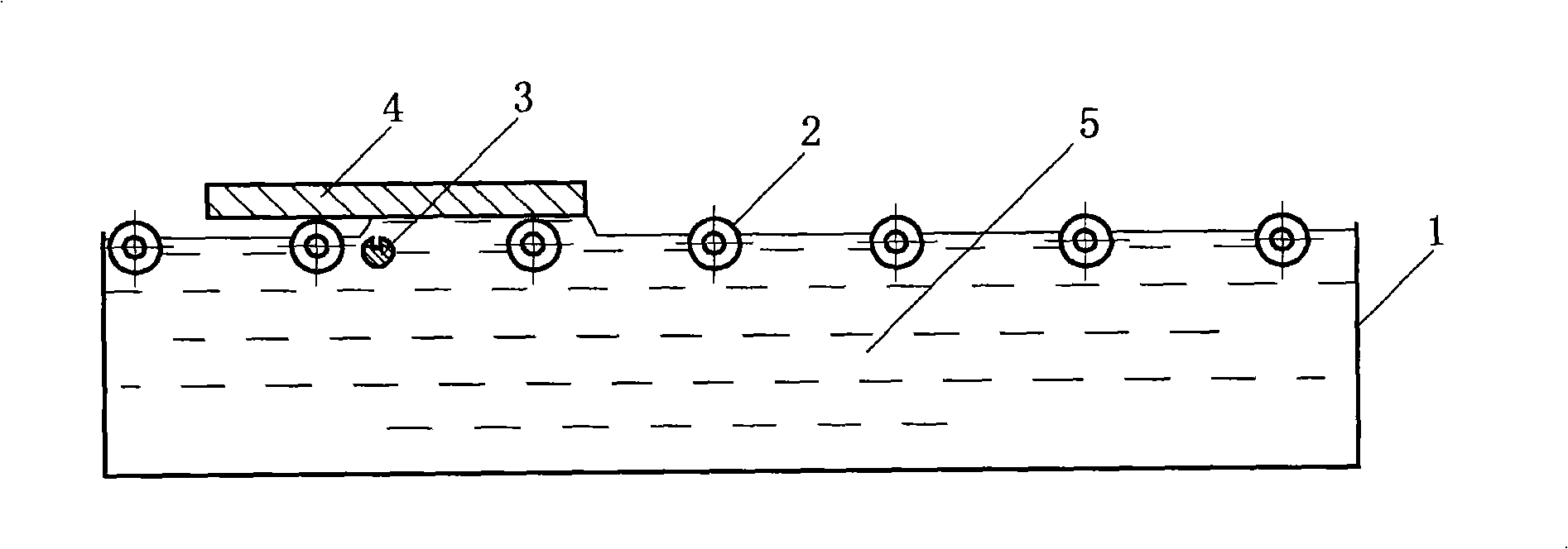
[0064] The chemical solution is a mixed solution of nitric acid and hydrofluoric acid. The injection device uses a nozzle and is fixed. The distance between the lower surface of the semiconductor substrate and the liquid surface of the chemical solution was 2 mm. When one edge of the semiconductor substrate moves over the nozzle, the nozzle sprays the chemical solution once. Then the lower surface of the semiconductor substrate is gradually wetted by the chemical solution under the action of surface tension as the semiconductor substrate continues to move. Throughout the process, the lower surface of the semiconductor substrate is in contact with the liquid level of the chemical solution in the chemical tank. After the treatment, the upper surface of the semiconductor substrate is not wetted by the chemical solution.

specific Embodiment 2

[0065]The injection device adopts multiple nozzles and is fixed. The distance between the lower surface of the semiconductor substrate and the liquid surface of the chemical solution was 10 mm. When one edge of the semiconductor substrate moves above the nozzle, the nozzle starts to spray the hydrofluoric acid solution until the other edge of the semiconductor substrate moves above the nozzle and stops. The semiconductor substrate continues to move, and when one edge of the semiconductor substrate moves above the next nozzle, the nozzle starts to spray the hydrofluoric acid solution until the other edge of the semiconductor substrate moves above the next nozzle and stops. During the whole process, the lower surface of the semiconductor substrate is not in contact with the liquid level of the chemical solution in the chemical tank. After the treatment, the upper surface of the semiconductor substrate is not wetted by the chemical solution.

specific Embodiment 3

[0066] The chemical solution is an electroless nickel plating solution. The injection device uses a nozzle and is fixed. The distance between the lower surface of the semiconductor substrate and the liquid surface of the chemical solution was 0.1 mm. When an edge of the semiconductor substrate moves above the nozzle, the nozzle starts to spray the electroless nickel plating solution. Continue until the other edge of the semiconductor substrate moves above the nozzle and stop. Throughout the process, the lower surface of the semiconductor substrate is in contact with the liquid level of the chemical solution in the chemical tank. After the treatment, the upper surface of the semiconductor substrate is not wetted by the chemical solution.


PUM

PropertyMeasurementUnit
thicknessaaaaaaaaaa
thicknessaaaaaaaaaa

Abstract

The present invention belongs to semi-conductor manufacturing industry field. The present invention discloses especially chemical processing method and device of a novel semi-conductor substrate surface. The chemical processing method of the present invention placed the semi-conductor substrate on the top of the chemical solution by using a bracket, and between the lower surface of the semi-conductor substrate and the liquid level of the chemical solution has a certain distance, and injects the chemical solution to the lower surface of the semi-conductor substrate by the spraying apparatus, thereby the lower surface is executed the chemical processing. The device of the present invention includes a chemical groove for holding the chemical solution, a bracket for placing the semi-conductor substrate above the chemical solution, and a spraying apparatus for injecting the chemical solution to the lower surface of the semi-conductor substrate. The chemical processing method and device of the present invention can execute chemical processing only for certain surface of the semi-conductor substrate, while no need protection for another surface.

Description

technical field [0001] The present invention relates to a technology for chemically treating a semiconductor substrate in the semiconductor manufacturing industry, in particular to a method for performing wet chemical treatment on a semiconductor substrate in the field of preparing semiconductor solar cells; more specifically, it involves performing wet chemical treatment on a certain surface of a semiconductor substrate The method of processing. Background technique [0002] Treating the surface of a semiconductor substrate with a chemical solution is a common process in the semiconductor manufacturing industry. For example, a surface etching process and a cleaning process are performed on the semiconductor substrate. Generally, the above wet chemical treatment process is carried out by immersing the semiconductor substrate in a chemical solution. In this case, wet chemical treatment is performed on both surfaces of the semiconductor substrate. [0003] However, in the i...

Claims


Application Information

Patent Timeline
Patent Type & Authority Applications(China)
IPC IPC(8): H01L21/306C23F1/24
CPCH01L21/67086H01L21/30604H01L21/67057H01L21/302H01L21/306
Inventor 季静佳覃榆森施正荣
Owner WUXI SUNTECH POWER CO LTD
Why Eureka
Try Eureka