Magnetic multilayer film with geometrical shape and preparation method and application thereof
A geometric shape and multi-layer film technology, applied in the application of magnetic film to substrate, magnetic layer, magnetic recording, etc., can solve the problems of bit layer reversal field and power consumption reduction
- Summary
- Abstract
- Description
- Claims
- Application Information
AI Technical Summary
Problems solved by technology
Method used
Image
Examples
Embodiment 1
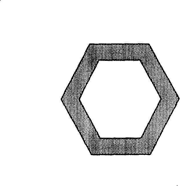
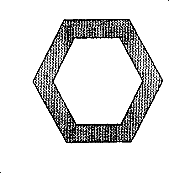
[0099] A non-pinning regular hexagonal closed ring magnetic multilayer film was prepared by microfabrication.
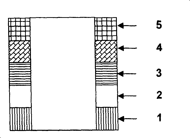
[0100] On high-vacuum magnetron sputtering equipment, 1mm thick SiO after cleaning by conventional methods 2 / Si substrate, using the conventional coating method to sequentially deposit Au with a thickness of 2nm as the lower buffer conductive layer 1, Co with a thickness of 3nm as the hard magnetic layer 2, Cu with a thickness of 1nm as the intermediate layer 3, and Co with a thickness of 1nm. As the soft magnetic layer 4 and Ru with a thickness of 4 nm as the capping layer 5 . The growth conditions of the above-mentioned magnetic multilayer film: prepared vacuum: 5×10 -7 Pa; high-purity argon gas pressure for sputtering: 0.07 Pa; sputtering power: 120 watts; sample holder rotation rate: 20rmp; growth temperature: room temperature; rate; and when depositing the hard magnetic layer 2 and the soft magnetic layer 4, a 150Oe plane induced magnetic field was applied. ...
Embodiment 2~7
[0102] According to the same method as in Example 1, a non-pinning regular pentagonal closed-loop magnetic multilayer film was prepared by microprocessing. The materials and thicknesses of each layer of the magnetic multilayer film are listed in Table 1.
[0103] Table 1. The structure of the non-pinning regular pentagonal closed ring magnetic multilayer film prepared by the micromachining method of the present invention
[0104]
[0105]
Embodiment 8
[0107] Fabrication of Pinned Regular Hexagonal Closed Ring Magnetic Multilayers by Microfabrication
[0108] Using high vacuum magnetron sputtering equipment to clean 0.8mm thick Si / SiO by conventional methods 2 Au lower buffer conductive layer 1 with a thickness of 2nm, an IrMn antiferromagnetic pinning layer 8 with a thickness of 10nm, and a Co with a thickness of 3nm were sequentially deposited on the substrate. 90 Fe 10 Pinned magnetic layer 9; then deposited 1nm thick Al, and an insulating layer formed by plasma oxidation for 50 seconds was used as the intermediate layer 3; on the intermediate layer 3, deposited a thickness of 3nm Co 90 Fe 10 A soft magnetic layer 4 and an Au capping layer 5 with a thickness of 2 nm. The growth conditions of the above-mentioned magnetic multilayer film: prepared vacuum: 5×10 -7 Pa; high-purity argon gas pressure for sputtering: 0.07 Pa; sputtering power: 120 watts; sample holder rotation rate: 20rmp; growth temperature: room temperatu...
PUM
| Property | Measurement | Unit |
|---|---|---|
| width | aaaaa | aaaaa |
| thickness | aaaaa | aaaaa |
| thickness | aaaaa | aaaaa |
Abstract
Description
Claims
Application Information
 - R&D
- Intellectual Property
- Life Sciences
- Materials
- Tech Scout
- Unparalleled Data Quality
- Higher Quality Content
- 60% Fewer Hallucinations
Browse by: Latest US Patents, China's latest patents, Technical Efficacy Thesaurus, Application Domain, Technology Topic, Popular Technical Reports.
© 2025 PatSnap. All rights reserved.Legal|Privacy policy|Modern Slavery Act Transparency Statement|Sitemap|About US| Contact US: help@patsnap.com


