


Quick Research
Generate reliable direction feasibility study reports for your R&D in just a few steps.

Technical Q&A
Discover and master advanced knowledge NOW. Basics, ideas, possibilities, all at once.

Find Solutions
As an expert in R&D theories, this can generate solutions to your technical problems instantly.

Evaluate Feasibility
Analyze your overall solution with one click, know your potential R&D risks in advance.

Monitor Landscape
Get weekly tech updates, stay abreast of the latest tech innovations and key insights.
Oxide p-i-n junction device and method for producing the same
A technology of oxide and junction devices, which is applied in the manufacture of semiconductor/solid-state devices, semiconductor devices, electrical components, etc., can solve the problems that the characteristics of oxide materials cannot be fully utilized, and achieve diversification, simple preparation methods, and easy structures Effect
- Summary
- Abstract
- Description
- Claims
- Application Information
AI Technical Summary
Problems solved by technology
Method used
Image

Examples
Embodiment 1
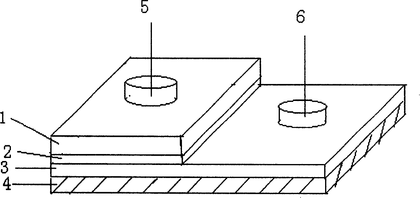
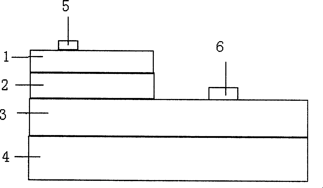
[0053] Figures 1A-1B A schematic oblique view and a side view of an embodiment of an all-metallic oxide p-i-n junction device fabricated according to the present invention are shown.
[0054] The oxide heterojunction device of this embodiment includes an STO substrate 4, a p-type oxide layer 3 formed on the STO substrate 4, to provide hole-type carriers, and a p-type oxide layer formed above the p-type oxide layer n-type oxide layer 1, to provide electron carriers, ferroelectric barrier layer 2 sandwiched between the p-type oxide layer 3 and the n-type oxide layer 1; the ferroelectric The barrier layer 2 is an oxide ferroelectric material Ba 1-e Sr e TiO 3 , the p-type oxide layer 3 is La 1-y Sr y MnO 3 , the n-type oxide layer 1 is La 2-a Ce a CuO 4 . The n-type oxide layer and the ferroelectric barrier layer are etched to 1 / 3 to 2 / 3 of the area by ion etching, and formed on the p-type oxide layer 3 and the n-type oxide layer 1 respectively A p-type oxide layer nob...
Embodiment 2
[0069] 5. After completing steps 1 to 4 in Example 1, apply a uniform layer of photoresist on the surface of the multilayer film using a coater. A photoresist mask was prepared on the multilayer film by using a glass-based mask.
[0070] 6. Using DC magnetron sputtering equipment, in the mode of DC sputtering, a layer of precious metal Ag is plated on the multilayer film.
[0071] 7. Clean the Ag-plated multilayer film with acetone. The photoresist and the Ag on the part of the photoresist mask pattern will be washed off by the acetone solution, and there is no photoresist mask. Ag will remain as pad.
[0072] 8. Using indium as the solder, solder the conductive leads to the solder pads at the terminals of the p-type oxide layer and the n-type oxide layer respectively.
Embodiment 3
[0074] 1. First, in the vacuum coating equipment, adjust the temperature to 680°C, and the vacuum degree of the back and bottom to be 5×10 -5 Pa; in a pure oxygen environment with a deposition pressure of 30Pa, use SrTiO 3 , MgO or LaAlO 3 as the substrate, on which the p-type metallic perovskite manganese oxide La 1-y Sr y MnO 3 , the La 1-y Sr y MnO 3 Layer thickness 200nm, ferroelectric oxide Ba 1-e Sr e TiO 3 Barrier layer 50nm and electronic oxide La 2-x Ce x CuO 4 n-type layer 200nm, made of multi-layer film;
[0075] Other steps are the same as the 2nd, 3rd, 4th, 5th, 6th steps among the embodiment 1.
PUM
| Property | Measurement | Unit |
|---|---|---|
| Thickness | aaaaa | aaaaa |
| Thickness | aaaaa | aaaaa |
| Thickness | aaaaa | aaaaa |
Abstract
Description
Claims
Application Information
 - R&D Engineer
- R&D Manager
- IP Professional
- Industry Leading Data Capabilities
- Powerful AI technology
- Patent DNA Extraction
Browse by: Latest US Patents, China's latest patents, Technical Efficacy Thesaurus, Application Domain, Technology Topic, Popular Technical Reports.
© 2024 PatSnap. All rights reserved.Legal|Privacy policy|Modern Slavery Act Transparency Statement|Sitemap|About US| Contact US: help@patsnap.com