Stripping preparation method of graphics platinum/titanium metal thin film
A titanium metal and patterning technology, applied in semiconductor devices and other directions, can solve the problems of poor adhesion between metal films and substrates, and achieve the effects of good adhesion, reduced difficulty and simple equipment
- Summary
- Abstract
- Description
- Claims
- Application Information
AI Technical Summary
Problems solved by technology
Method used
Image
Examples
Embodiment 1
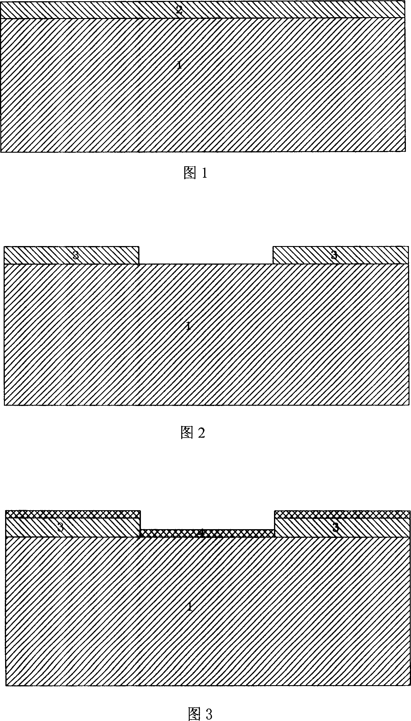
[0033] 1) Clean the silicon substrate
[0034] Cleaning the silicon substrate 1 with an acid cleaning solution or an alkaline cleaning solution respectively, and then rinsing it with deionized water;
[0035] 2) Preparation of zinc oxide sacrificial layer
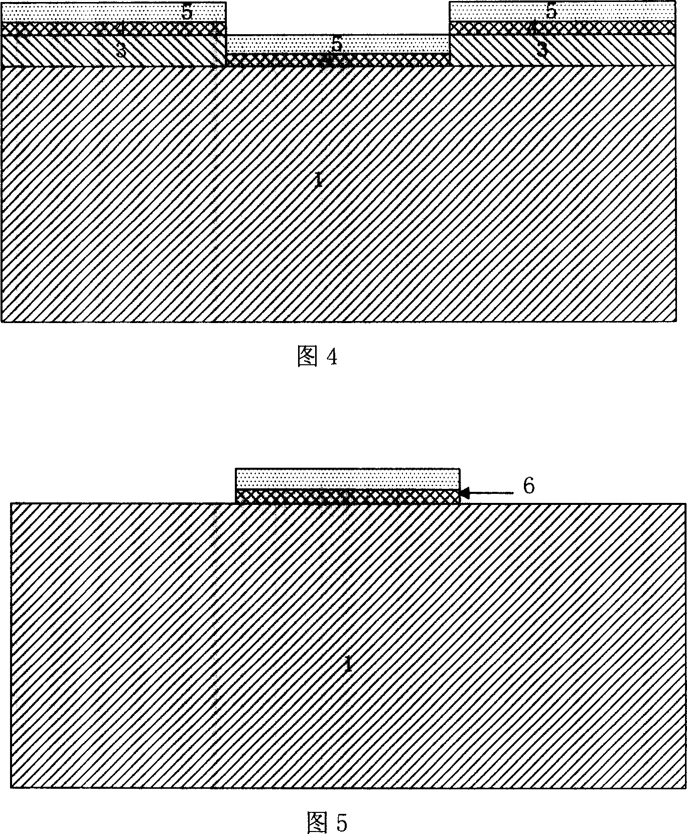
[0036] Using radio frequency sputtering equipment, prepare a 0.01 μm zinc oxide sacrificial layer 2 on the cleaned substrate 1; coat a positive photoresist on the surface of the zinc oxide 2, and use a negative version of the Pt / Ti metal film pattern to align the positive photoresist Resist photolithography exposure, using phosphoric acid as an etchant to wet pattern the sacrificial layer 3;
[0037] 3) Preparation of Ti metal film
[0038] Prepare a 0.05 μm Ti metal thin film layer 4 on the patterned sacrificial layer 3 by ion plating, and during the preparation process of the Ti metal thin film layer 4, the substrate 1 is heated to 150° C.;
[0039] 4) Preparation of Pt metal thin film
[0040] A 0.2 μm Pt metal thin ...
Embodiment 2
[0044] 1) Clean the potassium nitride substrate
[0045] Cleaning the potassium nitride substrate 1 with an acid cleaning solution or an alkaline cleaning solution respectively, and then rinsing it with deionized water;
[0046] 2) Preparation of zinc oxide sacrificial layer
[0047] Using DC sputtering equipment, prepare a 5 μm zinc oxide sacrificial layer 2 on the cleaned substrate 1; apply a negative photoresist on the surface of the zinc oxide sacrificial layer 2, and use the positive photoresist of the Pt / Ti metal thin film pattern Photolithographic exposure of the resist to form a sacrificial layer photoresist pattern; using phosphoric acid as an etching solution to wet-etch the patterned sacrificial layer 3;
[0048] 3) Preparation of Ti metal film
[0049] Prepare a 0.01 μm Ti metal thin film 4 on the patterned sacrificial layer 3 by using ion plating equipment, and the heating temperature of the substrate is 250°C;
[0050] 4) Preparation of Pt metal thin film
[...
Embodiment 3
[0055] 1) Clean the potassium arsenide substrate
[0056] Cleaning the potassium arsenide substrate 1 with an acid cleaning solution or an alkaline cleaning solution respectively, and then rinsing it with deionized water;
[0057] 2) Preparation of zinc oxide sacrificial layer
[0058] Coat positive photoresist on the silicon substrate 1 surface, utilize the negative version of Pt / Ti metal thin film pattern to positive photoresist photolithography exposure, or coat negative photoresist on the silicon substrate 1 surface, utilize The positive version of the Pt / Ti metal thin film pattern is exposed to the negative photoresist to form a photoresist pattern of the sacrificial layer;
[0059]Using radio frequency sputtering equipment, prepare a 10 μm zinc oxide sacrificial layer 2 on the substrate 1; use a conventional lift-off technique to pattern the sacrificial layer 3;
[0060] 3) Preparation of Ti metal film
[0061] A 0.1 μm Ti metal thin film 4 is prepared on the patterne...
PUM
| Property | Measurement | Unit |
|---|---|---|
| thickness | aaaaa | aaaaa |
| thickness | aaaaa | aaaaa |
Abstract
Description
Claims
Application Information
 - R&D
- Intellectual Property
- Life Sciences
- Materials
- Tech Scout
- Unparalleled Data Quality
- Higher Quality Content
- 60% Fewer Hallucinations
Browse by: Latest US Patents, China's latest patents, Technical Efficacy Thesaurus, Application Domain, Technology Topic, Popular Technical Reports.
© 2025 PatSnap. All rights reserved.Legal|Privacy policy|Modern Slavery Act Transparency Statement|Sitemap|About US| Contact US: help@patsnap.com


