High power laser diode driver
A laser diode and driver technology, applied in lasers, laser parts, semiconductor lasers, etc., can solve the problems of laser diode damage, no protection measures, and endangering the safe use of devices.
- Summary
- Abstract
- Description
- Claims
- Application Information
AI Technical Summary
Problems solved by technology
Method used
Image
Examples
Embodiment 1
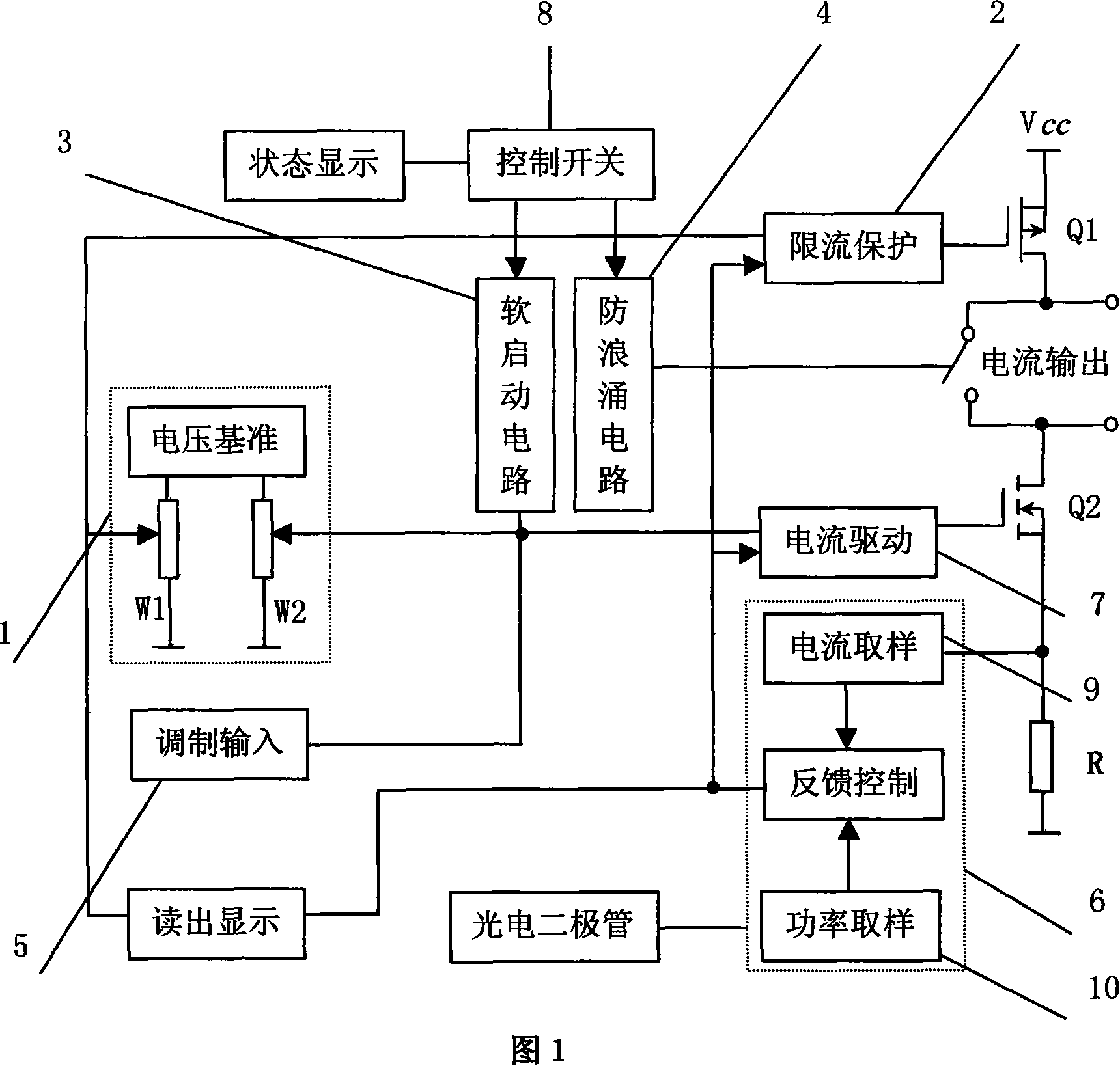
[0021] The functional block diagram of the driver voltage-controlled current source is shown in Figure 1. The voltage reference circuit 1 is composed of a voltage reference LM336-2.5 and a 9.1 kohm resistor, which provides an accurate and stable reference voltage for the circuit to control the output current and preset limit current. Potentiometer W1 is used to adjust the limit current, and potentiometer W2 is used to adjust the output current. The current limiting protection circuit 2 ensures that the output current does not increase when it reaches the limiting current, and maintains the set current unchanged. The current drive circuit 7 converts the control voltage into an output current. The high-power semiconductor device Q1 provides driving current for the laser diode, and the high-power semiconductor device Q2 can be a Darlington transistor or a field effect transistor. The present invention uses a power MOS transistor IRF530. When a large current drive is required, m...
Embodiment 2
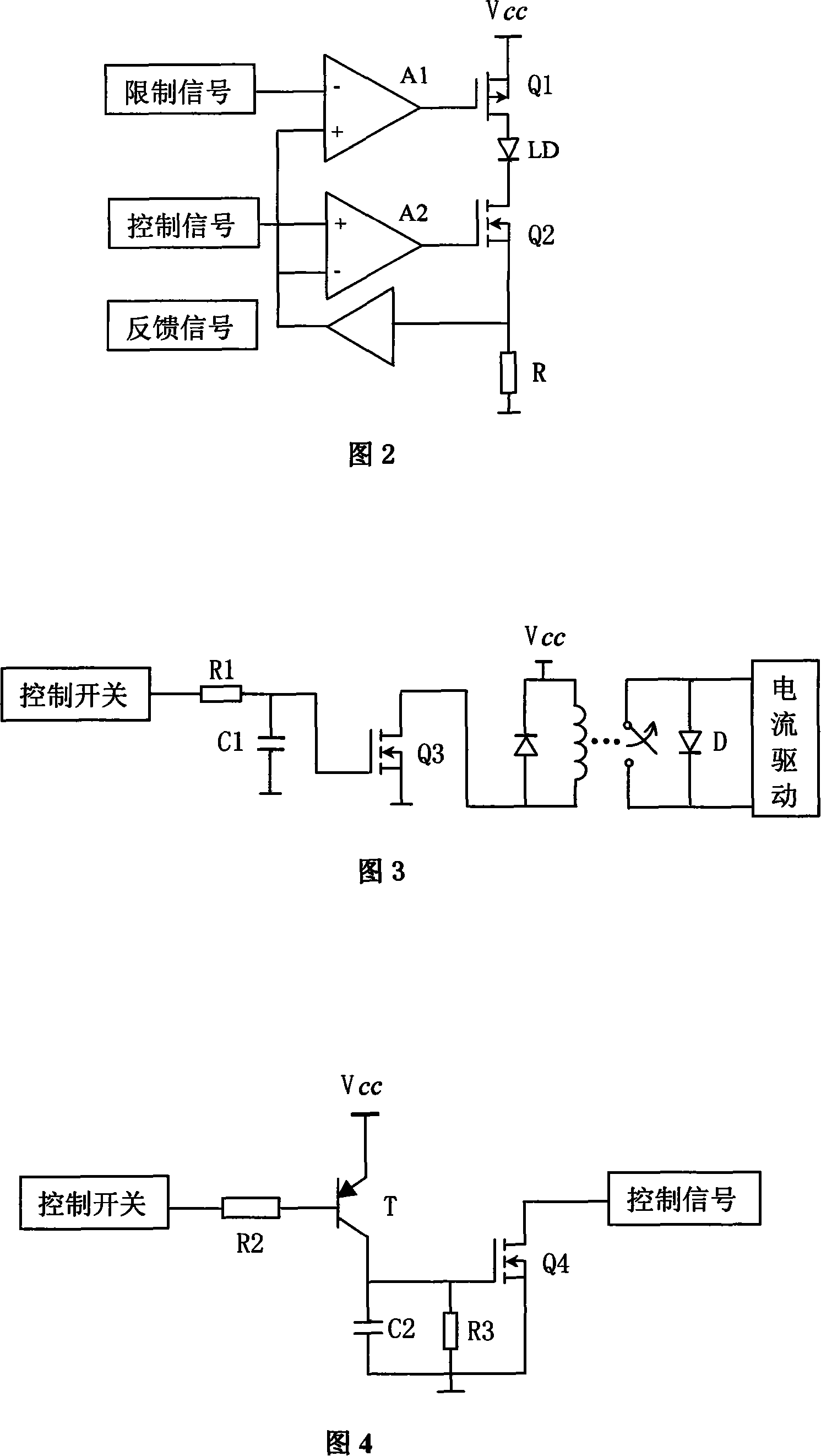
[0023] The block diagram of the current limiting protection circuit is shown in Figure 2. The circuit includes a P-channel enhanced field effect transistor Q1 and an N-channel enhanced field effect transistor Q2; the gates of the field effect transistors Q1 and Q2 are connected to the operational amplifiers A1 and A2 respectively; the drain of Q1 is connected to the laser diode LD The anode of Q2 is connected to the cathode of the laser diode LD; the source of Q1 is connected to the working power supply V CC The source of Q2 is connected to the sampling resistor R; the limit signal output by the potentiometer W1 is connected to the inverting terminal of the operational amplifier A1, and the control signal output by the potentiometer W2 is connected to the non-inverting terminal of the operational amplifier A2, which comes from the sampling resistor R The feedback signal is connected to the non-inverting terminal of the operational amplifier A1 and the inverting terminal of the...
Embodiment 3
[0027] The block diagram of anti-surge circuit is shown in Figure 3. The circuit includes an RC charging circuit composed of R1 and C1, an N-channel enhanced field effect transistor Q3, and a normally closed solid-state relay. The gate of the field effect transistor Q3 is connected to the resistors R1 and C1, the other end of C1 is grounded, the drain of the field effect transistor Q3 is connected to the relay, and the source of the field effect transistor Q3 is grounded. The model of the field effect transistor Q3 may be 2sk1458.
[0028] The working principle of the circuit is: the anode and cathode of the laser diode LD are connected in parallel with the two normally closed terminals of the relay, so the cathode and anode of the LD are short-circuited and protected. When the driver is turned on, if the control switch is not turned on, the LD is still short-circuited. Only after the control switch 8 is turned on, the normally closed end of the relay is opened after a delay ...
PUM
 Abstract
Description
Claims
Application Information
 - R&D
- Intellectual Property
- Life Sciences
- Materials
- Tech Scout
- Unparalleled Data Quality
- Higher Quality Content
- 60% Fewer Hallucinations
Browse by: Latest US Patents, China's latest patents, Technical Efficacy Thesaurus, Application Domain, Technology Topic, Popular Technical Reports.
© 2025 PatSnap. All rights reserved.Legal|Privacy policy|Modern Slavery Act Transparency Statement|Sitemap|About US| Contact US: help@patsnap.com


