
Turnable capacitor and switch using MEMS with phase change material

a technology of phase change material and turnable capacitor, which is applied in the field of mems, can solve the problems of limited tunability and accuracy of beam, shape memory alloy, and constant temperature for actuation

Inactive Publication Date: 2011-02-17
NXP BV
View PDF7 Cites 30 Cited by
  • Summary
  • Abstract
  • Description
  • Claims
  • Application Information

AI Technical Summary

Benefits of technology

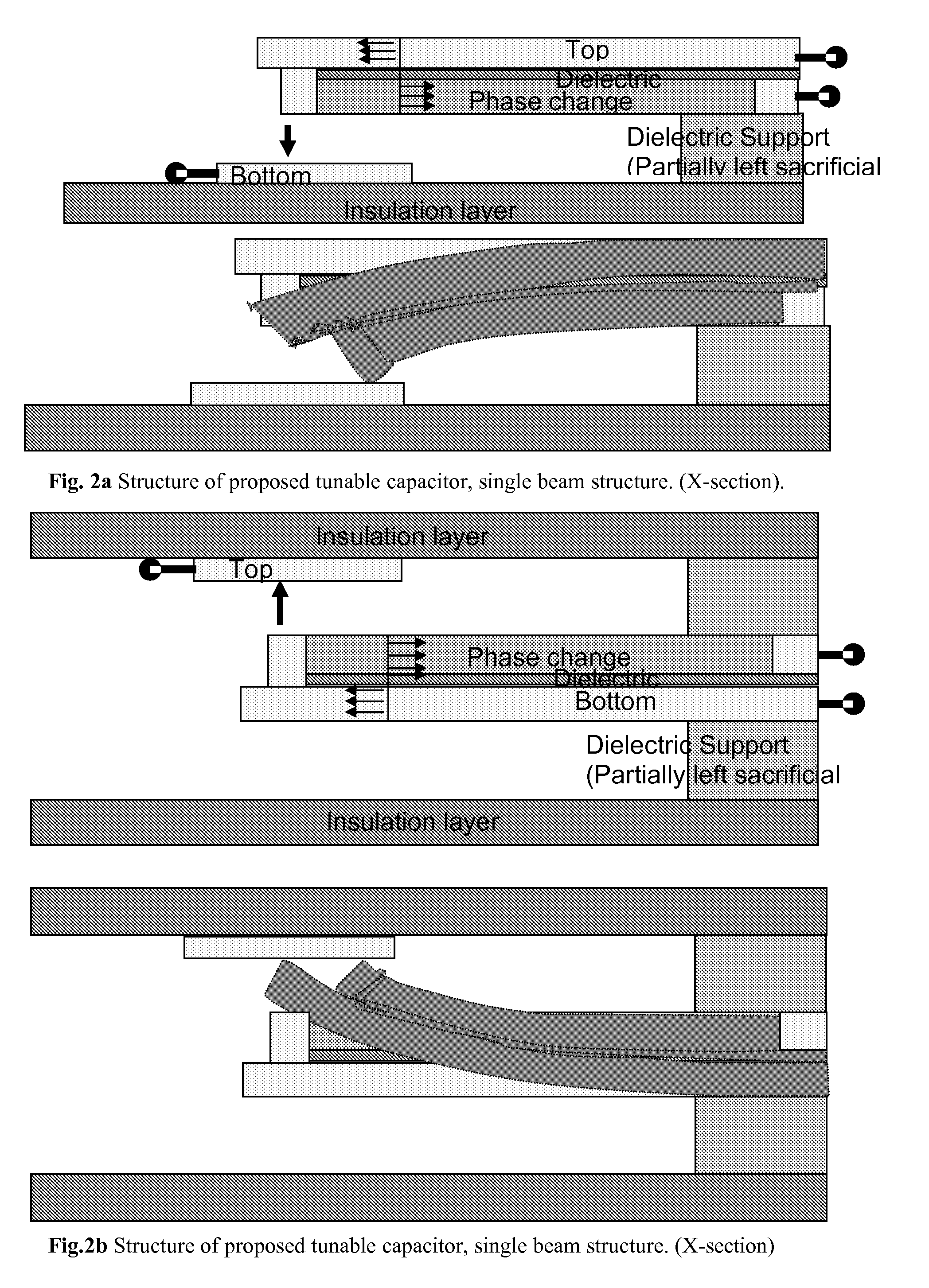
[0019]The present MEMS itself is regarded to function as a micro-actuator, being of a small size and implementing a process. As such it can be used in a switch, in a tunable capacitor, or as a mirror, if provided with a reflective layer, or combinations thereof Examples of MEMS structures are given in the drawings. It is noted that in fact the MEMS may be smaller than one micron, and therefore may also refer to a Nano type MEMS, also referred to as NEMS. A NEMS has advantages in terms of heat dissipation, being better if the NEMS is relatively smaller. As such, a further advantage is that a NEMS or a MEMS is easily integrated in CMOS technology.
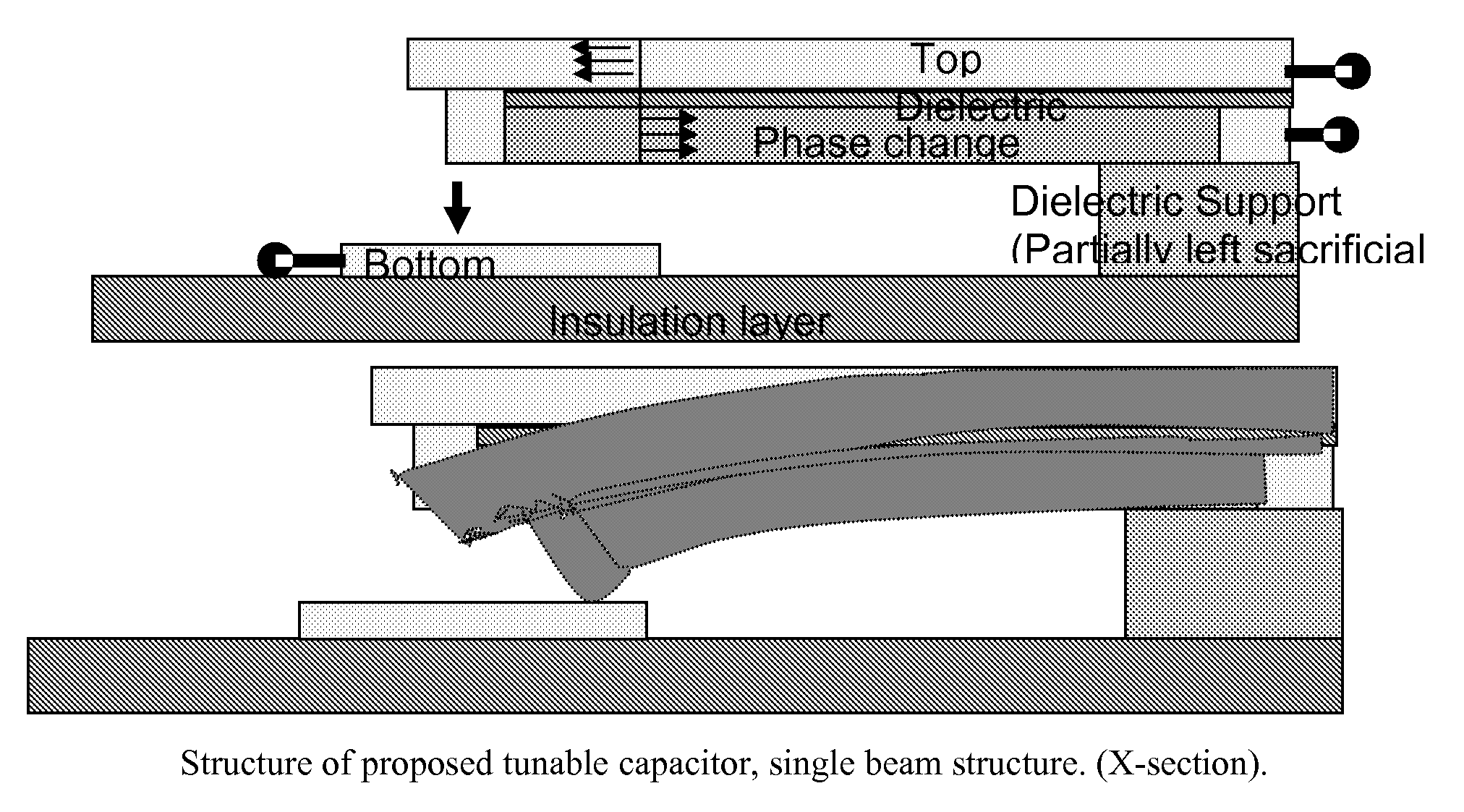
[0024]The phase change is preferably accomplished by applying an electrical current, which current causes the present phase change material to heat up, or by absence of said current, to cool down. The phase change results in a thermodynamically metastable or stable situation of the material, i.e. no phase change will take place by itself within a normal applicable time limit, such as minutes, or hours, or even years. As a result of actuation the volume of the present phase change material (PCM) will have changed. The present process is well controllable, by applying an electrical current which heats up the PCM to the required temperature, or by cooling. Furthermore, the present process is relatively quick, i.e. it takes place within a few microseconds. Adequate design allows for even shorter switching times. Examples of designs are given in the drawings. Therewith, switching times in the order of a few microseconds have been achieved. In other words, the present invention refers to a bi-stable actuation. It means that no electrical voltage is needed to maintain the position of the beam. An on current pulse is enough for that purpose. A (bi-)stable actuation is therefore very simple. A continuous actuation is possible by e.g. partial crystallization. It may also be achieved by segmenting the phase change layer and actuating a part of the beam, for instance by a multi-step actuation, for instance leading to multiple positions of the beam, or for instance leading to a stepped capacitor.
[0030]a high tunability, which may depend on material composition, such as having an εmax / εmin of more than 5, preferably more than 10, such as more than 20, or even more than 50, such as more than 100;
[0033]it is possible to control temperature. In the present invention the temperature of the beam (comprising a phase change material) is controlled by applying a current through the material for the beam. Further, a same or similar scheme for controlling temperature for the system may be used, wherein an array present can be used as a heater, allowing a high accuracy and reliability of the present tunable capacitor. It is noted that typically electrical properties are in the present respect detrimentally affected by temperature, for instance, electrical resistivity of metals increases with temperature, while the resistivity of semiconductors decreases with increasing temperature in general. Therefore, controlling temperature can provide an accurate electrical response, independent of circumstances, e.g. one of a resistor or capacitor present may be a temperature sensor, as shown in e.g. FIG. 4.
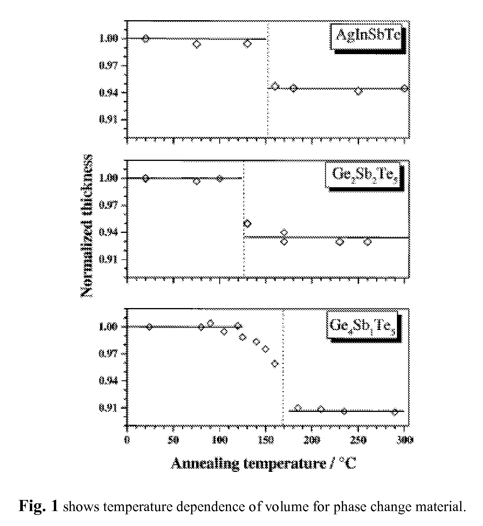
[0035]In a preferred embodiment the present invention relates to a semiconductor device, wherein the phase change material comprises a Group V and Group VI element, preferably a composition comprising Sb-M, wherein M being one or more elements selected from the group of Ge, In, Ag, Ga, Te, Zn, Sn, for instance; Ag5.5In6.5Sb59Te29, Ge0.08-0.4Sb0.1-0.33Te0.5-0.66, Ge2Sb2Te5, Ge1Sb2Te4, Ge1Sb4Te7 and Ge4SbiTe5, and combinations thereof. These materials have a large volume change, such as more than 5%, which volume change is achieved at relatively low temperatures, e.g. around 150° C. Furthermore, the phase transition of these materials is well controlled, e.g. by applying an electrical current which current forms heat. It is envisaged that also any phase change material, which can provide a high volume change at a temperature being close enough to room temperature, such as organic or polymer material, may be used, as well as combinations thereof.

Problems solved by technology

Therefore the beam has a limited tunability and limited accuracy.
Shape memory alloys have the disadvantage that they must be kept at a required temperature for actuation.
First, a high tunability of the MEMS is not possible.
Also, prior art capacitors and MEMS have a relatively large size.
Such capacitors further typically do not allow a control of temperature.
Next, a combination of electric and thermal tuning is not possible.

Method used


Image

  • Turnable capacitor and switch using MEMS with phase change material
  • Turnable capacitor and switch using MEMS with phase change material
  • Turnable capacitor and switch using MEMS with phase change material

Examples


Embodiment Construction

[0018]In a first aspect the invention relates to a semiconductor device comprising a MEMS, a first electrode, a second electrode, and a volume forming a beam comprising a phase change material, wherein the volume preferably comprises a dielectric material in contact with the phase change material and preferably comprises a conducting layer, wherein the device is arranged to electrically and controllably change the volume of the phase change material by going from one phase to another, thereby changing the volume by 5-25%, preferably higher than 9%, such as higher than 15%, wherein said change preferably occurs within a temperature range of 50-500° C., more preferably from 80-350° C., more preferably from 100-200° C., such as from 130-170° C.

[0019]The present MEMS itself is regarded to function as a micro-actuator, being of a small size and implementing a process. As such it can be used in a switch, in a tunable capacitor, or as a mirror, if provided with a reflective layer, or combi...


PUM


Abstract

The present invention relates to a MEMS, being developed for e.g. a mobile communication application, such as switch, tunable capacitor, tunable filter, phase shifter, multiplexer, voltage controlled oscillator, and tunable matching network. The volume change of phase-change layer is used for a bi-stable actuation of the MEMS device. The MEMS device comprises at least a bendable cantilever, a phase change layer, and electrodes. A process to implement this device and a method for using is given.

Description

FIELD OF THE INVENTION[0001]The present invention relates to a MEMS, being developed for e.g. a mobile communication application, such as switch, tunable capacitor, tunable filter, phase shifter, multiplexer, voltage controlled oscillator, and tunable matching network. The volume change of phase-change layer is used for a bi-stable actuation of the MEMS device. The MEMS device comprises at least a bendable cantilever, a phase change layer, and electrodes. A process to implement this device and a method for using is given.[0002]An example of the prior art is a capacitive RF MEMS switch, which can gain relatively large change of capacitance, due to change of distance or area between electrodes. However, these require an actuator to be controlled and response is slow. Another example is a tunable capacitor using ferroelectric or paraelectric material. The dielectric constant of these materials can be tuned by applying an electric field. Although these have a quick response for the elec...

Claims


Application Information

Patent Timeline
IPC IPC(8): H01G7/00H01L29/93H01L21/02
CPCB81B3/0072B81B2201/0221H01H1/0094B81C2201/0167H01G5/18B81B2203/0118
Inventor FURUKAWA, YUKIKOREIMANN, KLAUSRENDERS, CHRISTINA ADRIANAVAN PIETERSON, LIESBETHLIU, JINJEDEMA, FRISO JACOBUS
Owner NXP BV
Learn More