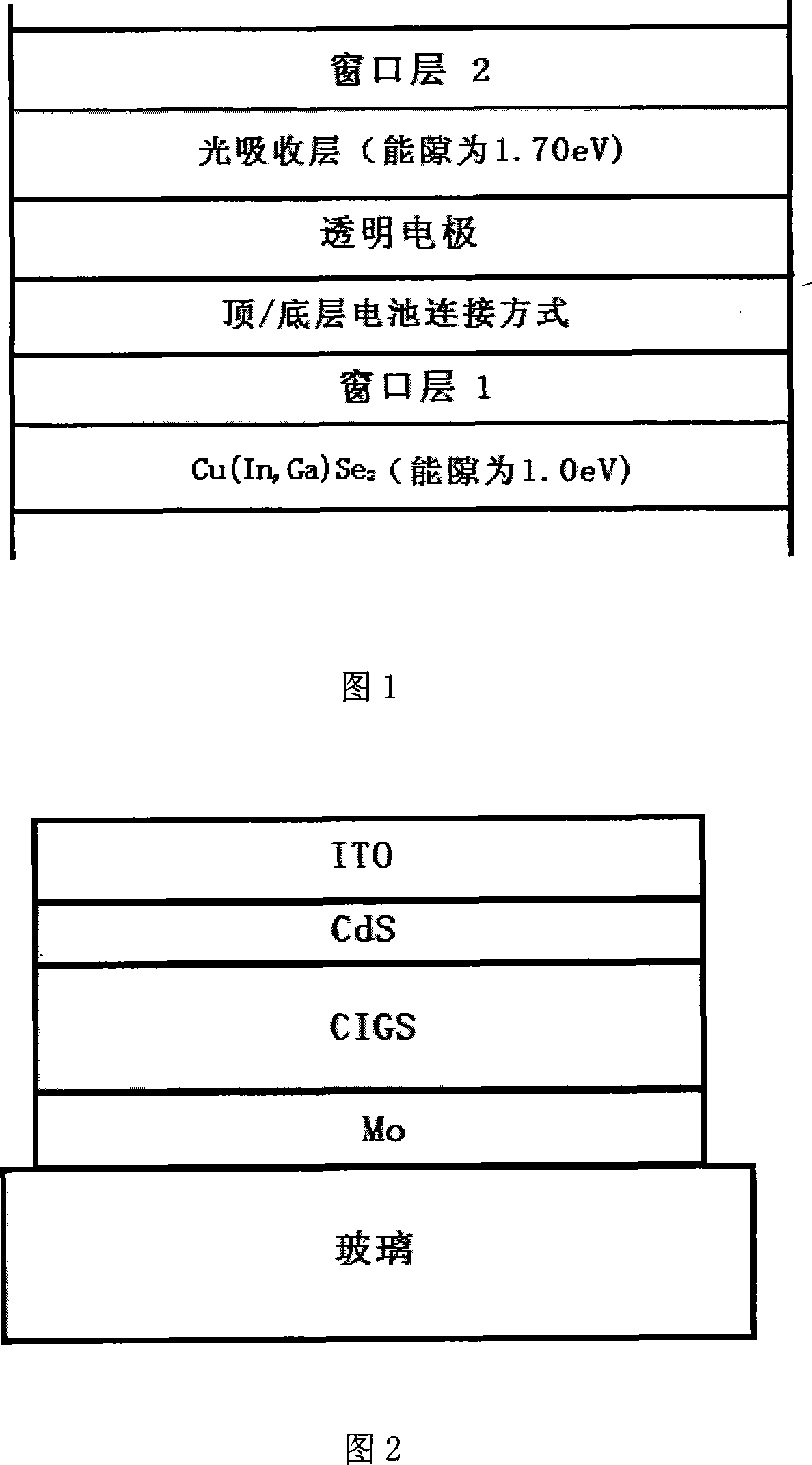
Highly-effective laminate solar battery and method for making same
A technology of solar cells and solar cells, applied in circuits, electrical components, photovoltaic power generation, etc., can solve problems such as inherent defects and limitations of stacked solar cells, improve quality and performance, avoid the influence of temperature-sensitive layers, The effect of overcoming the dilemma of high temperature process
- Summary
- Abstract
- Description
- Claims
- Application Information
AI Technical Summary
Problems solved by technology
Method used
Image
Examples
Embodiment 1
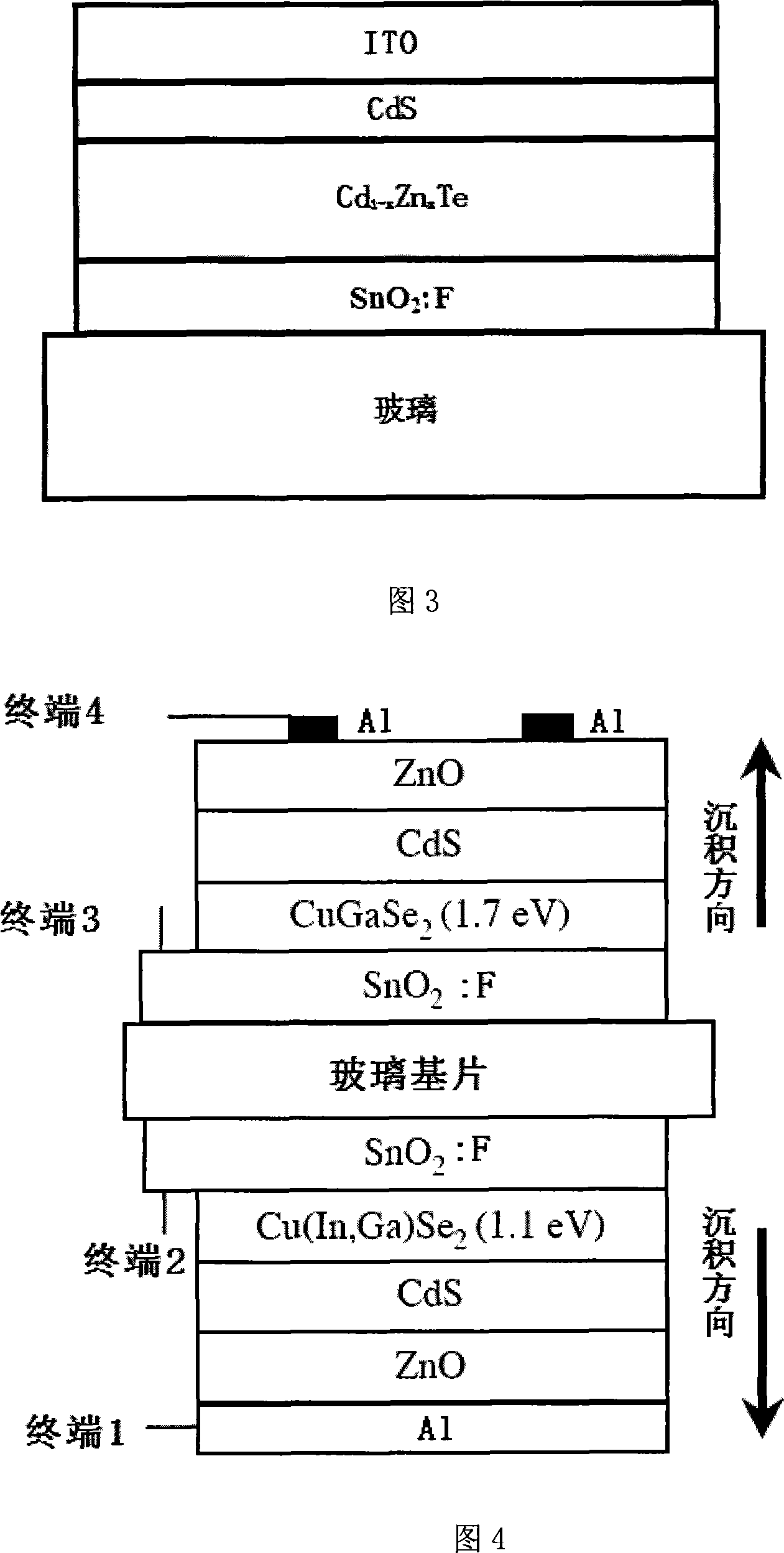
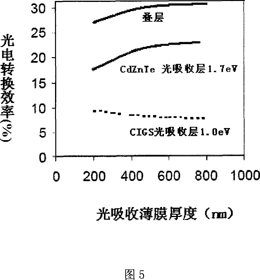
[0037] Embodiment 1: Preparation of CdZnTe / CIGS tandem solar cell
[0038] 1. Narrow bandgap Cu(In, Ga)Se 2 Fabrication of (CIGS) Thin Film Solar Cell
[0039] (1) According to the post-sputtering selenization method for making CIGS solar cells, a single-layer narrow-bandgap CIGS thin-film solar cell was prepared. (2) The glass substrate was ultrasonically cleaned with acetone, alcohol, and deionized water for 15 minutes respectively, and then dried with pure nitrogen. Use a magnetron sputtering system to sputter a layer of metal molybdenum of about 1 μm as the back electrode of the battery; (3) sputter a copper indium alloy target on the molybdenum film, coat a layer of about 0.6 μm copper indium prefabricated layer, and then Using two-step selenization, the first step of selenization temperature is 200°C, time 25mins, the second step selenization temperature is 450°C, time 25mins, to obtain a copper indium selenium thin film with an energy gap of 1.0eV, with a thickness of...
Embodiment 2
[0044] Example 2: CGS / CIGS tandem solar cell
[0045] According to the post-sputtering selenization method for making CIGS series solar cells, wide bandgap CGS and narrow bandgap CIGS thin film solar cells are prepared simultaneously. (1) A double-sided FTO glass substrate was ultrasonically cleaned with acetone, alcohol, and deionized water for 15 minutes, and then dried with nitrogen; (2) firstly, SnO 2 : On the F film layer, a copper-gallium prefabricated layer of about 0.6 μm is plated on the copper-gallium alloy target by sputtering, and then the double-sided FTO glass is coated with SnO 2 : Copper-indium alloy target is sputtered on the F film layer, and a layer of about 0.6 μm copper-indium prefabricated layer is plated. Finally, the copper-gallium prefabricated layer and the copper-indium prefabricated layer are selenized simultaneously by two-step method. The first step is to selenize the copper-indium prefabricated layer. The selenization temperature is 250°C for 30...
PUM
| Property | Measurement | Unit |
|---|---|---|
| Bandgap width | aaaaa | aaaaa |
| Thickness | aaaaa | aaaaa |
Abstract
Description
Claims
Application Information
 - Generate Ideas
- Intellectual Property
- Life Sciences
- Materials
- Tech Scout
- Unparalleled Data Quality
- Higher Quality Content
- 60% Fewer Hallucinations
Browse by: Latest US Patents, China's latest patents, Technical Efficacy Thesaurus, Application Domain, Technology Topic, Popular Technical Reports.
© 2025 PatSnap. All rights reserved.Legal|Privacy policy|Modern Slavery Act Transparency Statement|Sitemap|About US| Contact US: help@patsnap.com


