Nonvolatile semiconductor storage device and method for manufacturing the same
一种非易失性、存储器件的技术,应用在半导体/固态器件制造、半导体器件、静态存储器等方向,能够解决不能抑制寄生晶体管、不能形成等问题,达到有利电荷保持特性的效果
- Summary
- Abstract
- Description
- Claims
- Application Information
AI Technical Summary
Problems solved by technology
Method used
Image

Examples
Embodiment approach 1
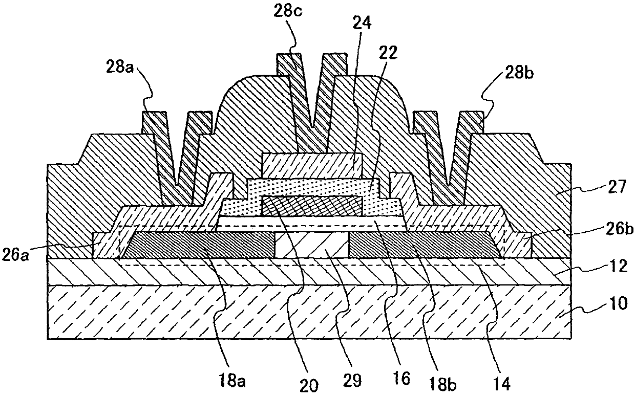
[0051] figure 1 The sectional view of is illustrating the main structure of the nonvolatile semiconductor memory device related to the present invention. figure 1 In particular, the main part of the non-volatile storage element is illustrated.
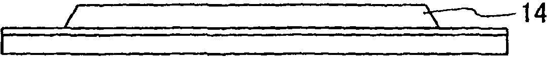
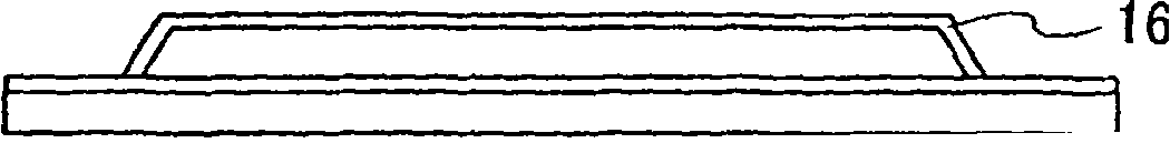
[0052] exist figure 1 Among them, reference numeral 10 denotes a substrate, 12 is a base insulating film, 14 is a semiconductor layer, 29 is a channel formation region, 18a and 18b are source regions or drain regions, and 16 is a first insulating film (also referred to as a tunnel insulating film). film), 20 is a floating gate electrode, 22 is a second insulating film (also called a control insulating film), 24 is a control gate electrode, 26a and 26b are conductive layers, 28a and 28b are electrically connected to the The source or drain electrodes of the source or drain regions 18a and 18b, 28c is a gate wiring electrically connected to the control gate electrode, and 27 is an insulating film for passivation.
[0053] exist f...
Embodiment approach 2
[0106] In this embodiment, structures different from figure 1 The structure of the nonvolatile memory element is shown in the method of manufacturing the nonvolatile memory element. In this embodiment, it will be described as Figure 11 The nonvolatile storage element shown. exist Figure 11 In the nonvolatile memory element shown, the control gate electrode 24 has sidewalls 300 .
[0107] exist Figure 11 12, a base insulating film; 14, a semiconductor layer; 29, a channel formation region; 18a and 18b, a source region or a drain region; 16, a first insulating film (also called a tunnel insulating film). 20 is a floating gate electrode; 22 is a second insulating film (also called a control insulating film); 24 is a control gate electrode; 300 is a side wall; 26a and 26b are conductive layers; 28a and 28b are through conductive layer 26a and 26b are connected to source or drain electrodes of the source or drain regions 18a and 18b; 28c is a gate wiring electrically conne...
Embodiment approach 3
[0122] In this embodiment, the combined Figure 14A and 14B , Figures 15A to 15D as well as Figure 16A and 16B Description is different from figure 1 and 11 The structure of the nonvolatile memory shown in the structure.
[0123] exist Figure 14A In the shown nonvolatile memory element, first impurity regions (source or drain regions) 306a and 306b, second impurity regions 307a and 307b, etc. are provided in the semiconductor layer 14, and the floating gate electrode 20 is composed of the first floating gate electrode 20a and second floating gate electrode 20b are formed, which are different from figure 1 and Figure 11 place of the structure shown.
[0124] in such as Figure 14A In the shown structure, a base insulating film 12 is formed on a substrate 10, and a semiconductor layer 14 having first impurity regions 306a and 306b, second impurity regions 307a and 307b, and a channel formation region 29 is formed on the base insulating film 12. . The first insu...
PUM
 Abstract
Description
Claims
Application Information
 - R&D
- Intellectual Property
- Life Sciences
- Materials
- Tech Scout
- Unparalleled Data Quality
- Higher Quality Content
- 60% Fewer Hallucinations
Browse by: Latest US Patents, China's latest patents, Technical Efficacy Thesaurus, Application Domain, Technology Topic, Popular Technical Reports.
© 2025 PatSnap. All rights reserved.Legal|Privacy policy|Modern Slavery Act Transparency Statement|Sitemap|About US| Contact US: help@patsnap.com