Illumination device
A lighting device and semiconductor technology, applied in the direction of electrical components, electrical solid devices, circuits, etc., can solve the problems of high cost and achieve the effect of reducing graininess
- Summary
- Abstract
- Description
- Claims
- Application Information
AI Technical Summary
Problems solved by technology
Method used
Image

Examples
Embodiment Construction
[0070] A first embodiment of the present invention will be described with reference to FIGS. 1 to 3 .
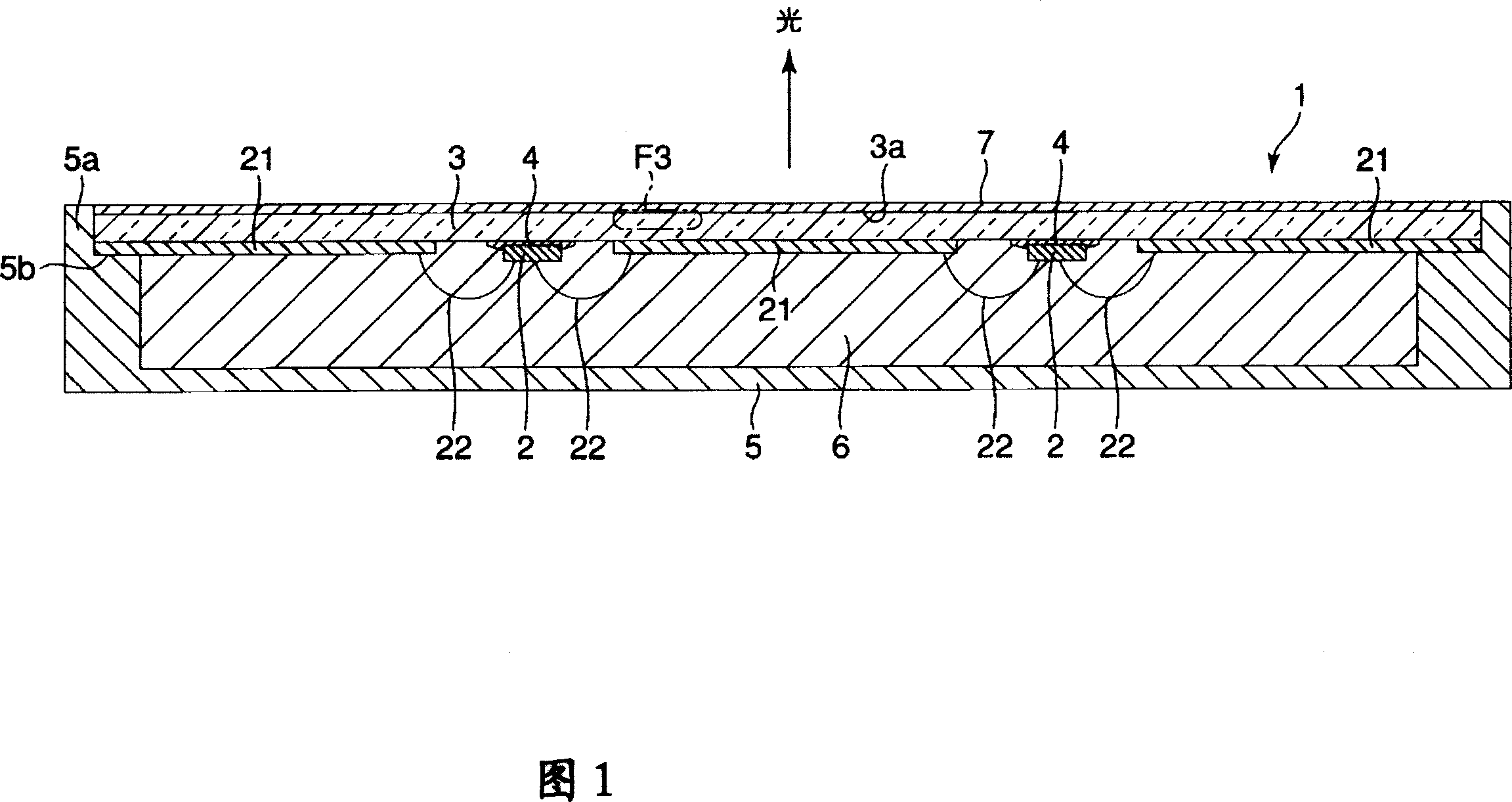
[0071] In FIG. 1 , reference numeral 1 denotes a lighting device in which an LED package is formed. The lighting device 1 includes a plurality of semiconductor light emitting elements 2 , a translucent substrate 3 , an adhesive layer 4 , a reflection member 5 , a sealing member 6 , and a phosphor layer 7 .
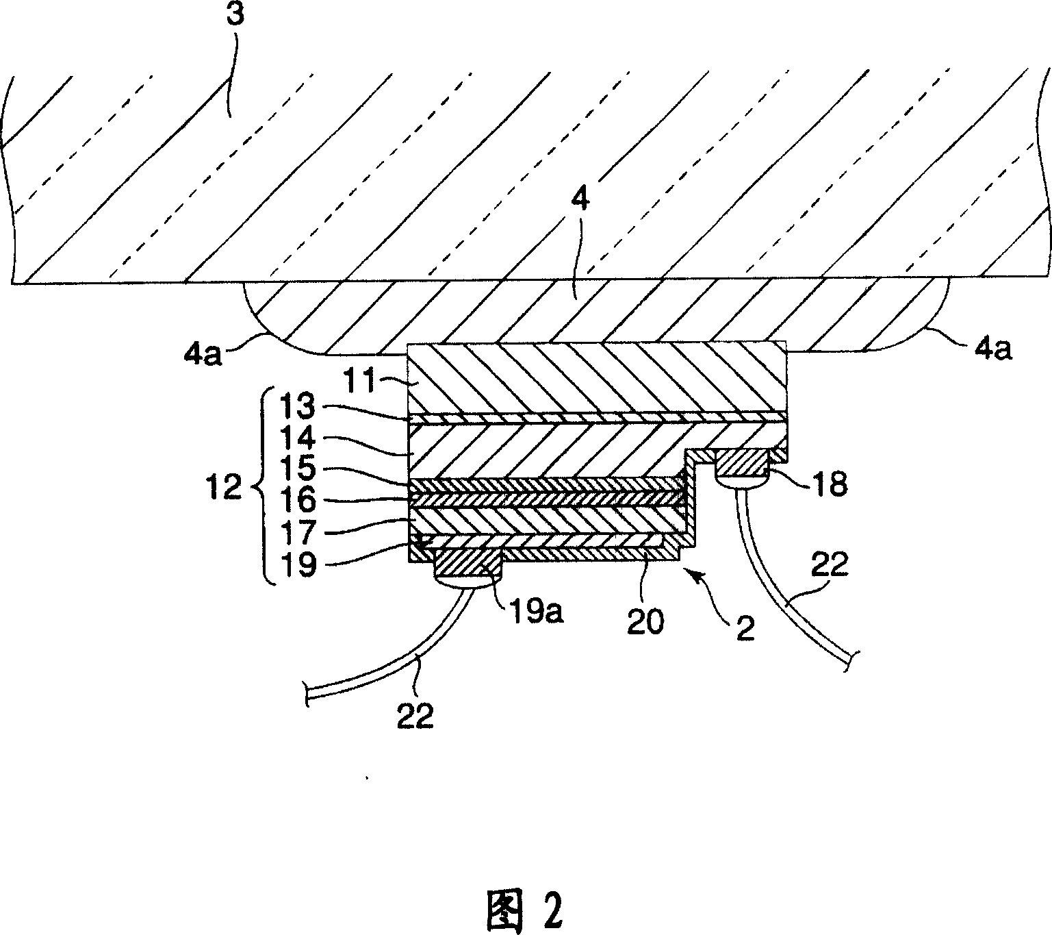
[0072] The semiconductor light-emitting element 2 is, for example, a two-wire LED chip formed using a nitride semiconductor, and is formed by laminating a semiconductor light-emitting layer 12 on the back surface of a light-transmitting, electrically insulating element substrate 11 . The element substrate 11 is made of, for example, a sapphire substrate.
[0073] As shown in FIG. 2, the semiconductor light emitting layer 12 is sequentially stacked with a buffer layer 13, an n-type semiconductor layer 14, a light emitting layer 15, a p-type clad layer (clad layer) 16 and...
PUM
 Abstract
Description
Claims
Application Information
 - R&D
- Intellectual Property
- Life Sciences
- Materials
- Tech Scout
- Unparalleled Data Quality
- Higher Quality Content
- 60% Fewer Hallucinations
Browse by: Latest US Patents, China's latest patents, Technical Efficacy Thesaurus, Application Domain, Technology Topic, Popular Technical Reports.
© 2025 PatSnap. All rights reserved.Legal|Privacy policy|Modern Slavery Act Transparency Statement|Sitemap|About US| Contact US: help@patsnap.com