Method for improving the performance of gallium nitride based field effect transistor

A gallium nitride base field and transistor technology, which is applied in semiconductor/solid-state device manufacturing, electrical components, circuits, etc., can solve the problem of affecting device stability and reliability, increasing gate reverse leakage current, and increasing electric field at the edge of gate metal and other problems, to achieve the effect of greatly increasing the gate reverse leakage current, reducing the surface state density, and reducing the leakage current

Inactive Publication Date: 2010-03-17
SEMICON MFG INT (SHANGHAI) CORP +1
View PDF4 Cites 5 Cited by
  • Summary
  • Abstract
  • Description
  • Claims
  • Application Information

AI Technical Summary

Problems solved by technology

[0014] 1. There are surface states and original oxide layers on the surface of AlGaN, and the concentration of surface states is not eliminated or reduced due to silicon nitride passivation. PECVD deposited silicon nitride is passivated, and the surface states and surface states that exist at the interface between AlGaN and silicon nitride The original oxide layer, so that there is still a certain degree of current collapse effect
[0015] 2. The original oxide layer existing on the surface of AlGaN makes the electric field at the edge of the gate metal increase significantly after silicon nitride passivation, so that the gate reverse leakage current increases to a large extent after silicon nitride passivation. This will seriously affect the breakdown voltage of the device and may reduce the power gain of the device to a large extent
[0016] 3. The original oxide layer and surface state existing at the interface of AlGaN and silicon nitride after passivation are characterized by instability, which seriously affects the stability and reliability of the device under the action of long-term high-frequency high-electric field stress

Method used


Image

  • Method for improving the performance of gallium nitride based field effect transistor
  • Method for improving the performance of gallium nitride based field effect transistor
  • Method for improving the performance of gallium nitride based field effect transistor

Examples


Embodiment Construction

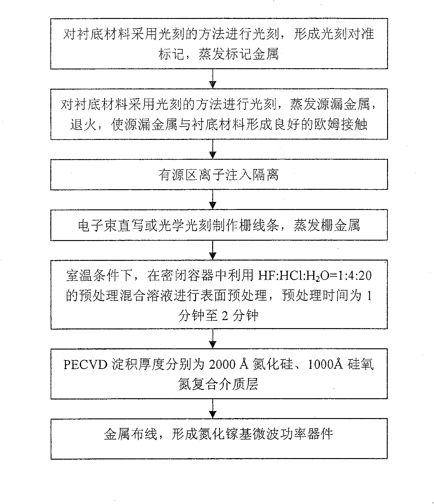
[0041] In order to make the object, technical solution and advantages of the present invention clearer, the present invention will be described in further detail below in conjunction with specific embodiments and with reference to the accompanying drawings.

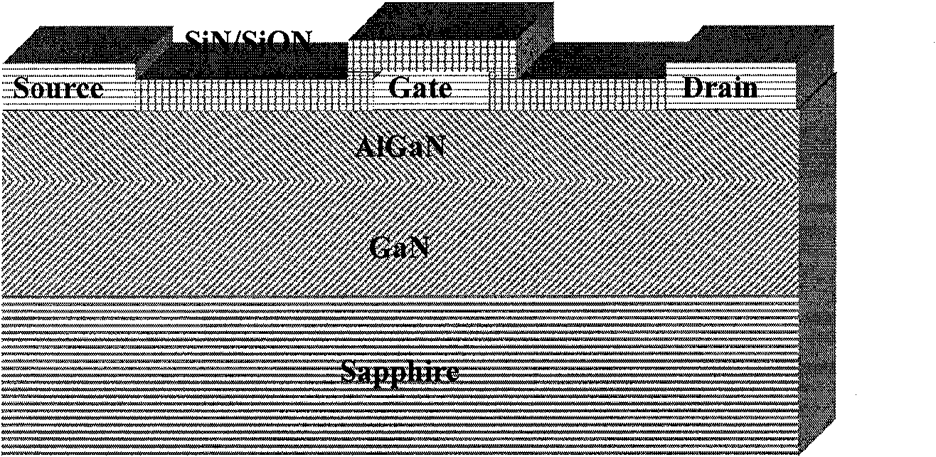
[0042] Such as figure 1 as shown, figure 1 It is a structural schematic diagram of a GaN-based field effect transistor based on the present invention, the GaN-based field effect transistor includes: a gate, a source and a drain on both sides of the gate; wherein, the gate, the source and the drain are located on the substrate On the aluminum gallium nitride (AlGaN) epitaxial layer on the top layer of the bottom material, ohmic contacts are formed between the source electrode and the AlGaN epitaxial layer, and between the drain electrode and the AlGaN epitaxial layer through annealing alloy. On the AlGaN epitaxial layer between the source electrode and the drain electrode, gate lines are fabricated by electron beam direct...


PUM

PropertyMeasurementUnit
sizeaaaaaaaaaa

Abstract

The invention relates to the technical field of production of wide bandgap semiconductor materials and devices and discloses a method for improving the performance of a GaN-based field-effect transistor, the method comprises: mixed pre-treatment solution is adopted to carry out the surface pre-treatment of the surface of a device before the passivation of the GaN-based field-effect transistor during the production process of the GaN-based field-effect transistor, then a compound dielectric layer of silicon nitride and oxygen-rich silicon nitride is deposited on the surface of the device afterthe surface pre-treatment, and the GaN-based field-effect transistor is passivated. The use of the method can solve a surface original oxide layer which is existed on the surface of AlGaN for a long time, eliminate the AlGaN surface state which is induced by the surface oxide layer, solve the surface state existing in an AlGaN and silicon nitride interface, the current collapse effect which is induced by the surface original oxide layer and the significant increase of the reverse gate leakage current caused by the conventional passivation and improve the stability and the reliability of GaN-based HEMT.

Description

technical field [0001] The invention relates to the technical field of manufacturing wide bandgap semiconductor material devices, in particular to a method for improving the performance of gallium nitride-based field effect transistors. Background technique [0002] Gallium nitride (GaN), as the third-generation wide-bandgap semiconductor material, has a large bandgap (3.4eV), a high breakdown voltage (3.3MV / cm), and a high two-dimensional electron gas concentration (>10 13 cm 2 ), high velocity of saturated electrons (2.8×10 7 cm / s) and other characteristics have received extensive attention internationally. At present, the high-frequency, high-voltage, high-temperature and high-power characteristics of GaN-based field-effect transistor (AlGaN / GaN HEMT) devices make them have great application prospects in microwave power devices. [0003] Although the performance of aluminum gallium nitride / gallium nitride (AlGaN / GaN) HEMT devices has made great progress in recent ye...

Claims


Application Information

Patent Timeline
Patent Type & Authority Patents(China)
IPC IPC(8): H01L21/335
Inventor 李诚瞻魏珂刘新宇刘键刘果果郑英奎王冬冬黄俊和致经
Owner SEMICON MFG INT (SHANGHAI) CORP
Why Eureka
Try Eureka