Silicon based LCD micro- display and method for forming same

A technology of microdisplay and liquid crystal on silicon, applied in the field of semiconductor, can solve the problems of difficult monolithic structure and large influence of adjacent units, and achieve the effect of small interference effect and small mutual influence

Active Publication Date: 2009-12-30
SEMICON MFG INT (SHANGHAI) CORP +1
View PDF3 Cites 0 Cited by
  • Summary
  • Abstract
  • Description
  • Claims
  • Application Information

AI Technical Summary

Problems solved by technology

[0005] The problem solved by the invention is that in the existing silicon-based liquid crystal microdisplay technology, the microreflector adopts a rectangular shape, which is not easy to be made into a monolithic structure, and at the same time, the influence between adjacent units is large

Method used


Image

  • Silicon based LCD micro- display and method for forming same
  • Silicon based LCD micro- display and method for forming same
  • Silicon based LCD micro- display and method for forming same

Examples


Embodiment Construction

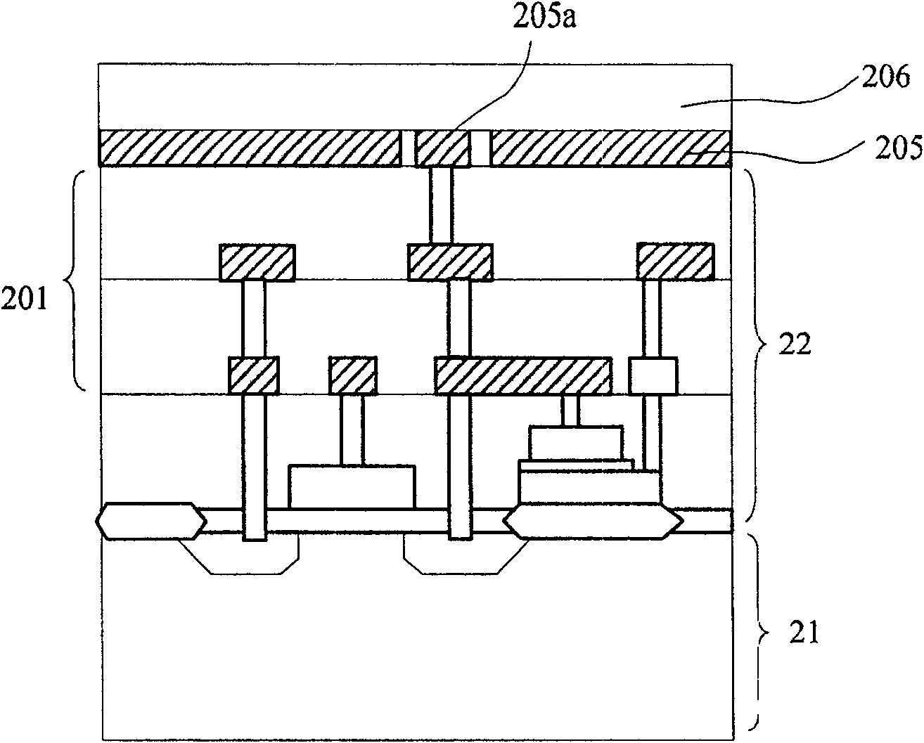
[0024] The essence of the present invention is to provide a silicon-based liquid crystal microdisplay and a method for forming the same. The microreflector of the silicon-based liquid crystal microdisplay is a honeycomb regular hexagon. The pixel switch circuit layer of the silicon-based liquid crystal microdisplay provided by the present invention The random memory composed of MOS transistors and capacitors can also be other forms of static random access memory circuits or pixel switch circuits composed of address selection diodes. The protection scope of the present invention should not be excessively limited here.

[0025] In the following, specific embodiments are described in detail according to the accompanying drawings to make the above-mentioned objectives and advantages of the present invention more clear:

[0026] First, a method for forming a silicon-based liquid crystal microdisplay unit is given. A pixel switch circuit layer and an intermetallic insulating layer are f...


PUM


Abstract

The invention relates to a formation method of a silicon-based liquid crystal micro-display, which comprises the following steps: a pixel switch circuit layer is formed on a silicon substrate; a light shielding layer and an intermetallic insulation layer are formed in turn on the pixel switch circuit layer; a metal reflection layer is formed on the insulation layer; and the metal reflection layer is etched to form a separated hexagonal micro-reflection mirror array. Accordingly, the invention provides a silicon-based liquid crystal micro-display. The micro-reflection mirrors of the invention are hexagon-shaped; since three micro-reflection mirrors border upon each other, the invention is easy to form a monolithic structure; and since the inner angle of the hexagon is 120 degrees, the shape is nearly a circle, the adjacent micro-reflection mirrors have smaller interaction due to the interference effect, thereby reducing the phenomenon of optical crosstalk.

Description

Technical field [0001] The invention relates to the field of semiconductors, in particular to a silicon-based liquid crystal microdisplay and a method for forming the same. Background technique [0002] In recent years, many new technologies have emerged in the liquid crystal (LCD) industry, among which the more popular technology is the Liquid Crystal on Silicon (LCOS) technology. LCOS (Liquid Crystal on Silicon) is a new type of reflective micro LCD projection technology. Its structure is to grow a transistor on a silicon substrate, use a semiconductor process to make a drive panel (also known as CMOS-LCD), and then pass through the transistor. Grinding technology is ground, and plated with aluminum as a micro-reflector to form a CMOS substrate. Then the CMOS substrate is bonded to the glass substrate containing the transparent electrode, and then liquid crystal is injected for packaging testing. [0003] Generally speaking, LCOS displays can be divided into two categories: thr...

Claims


Application Information

Patent Timeline
Patent Type & Authority Patents(China)
IPC IPC(8): G02F1/1362G02F1/136H01L21/822H01L27/04
Inventor 黄河高大为蒲贤勇
Owner SEMICON MFG INT (SHANGHAI) CORP
Why Eureka
Try Eureka