Preparation method of Zno back gate nano wire field effect tube
A technology of field effect tubes and nanowires, applied in semiconductor/solid-state device manufacturing, electrical components, circuits, etc., can solve problems such as inability to optimize device structure, inability to guide device process, etc., achieve low cost, save cost, and simple process easy effect
- Summary
- Abstract
- Description
- Claims
- Application Information
AI Technical Summary
Problems solved by technology
Method used
Image
Examples
Embodiment Construction
[0026] The present invention will be further described in detail below in conjunction with specific embodiments and with reference to the drawings.
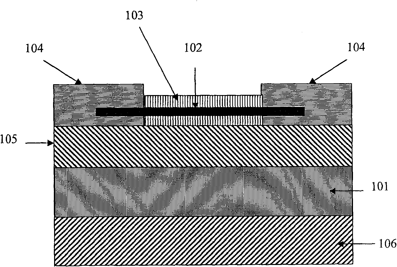
[0027] The present invention provides a method for preparing a ZnO back-gate nanowire field effect tube. The steps of the preparation method are as follows:
[0028] (1) In P ++ SiO growth on type Si substrate 101 2 Dielectric layer 105, glue coating, pre-baking, RIE primer, using cross or groove plate to lithography the substrate;
[0029] The SiO 2 The thickness of the dielectric layer 105 is 2000~ The glue is coated with positive glue 5214, the rotating speed is 3500 rpm when the glue is uniformed, and the glue thickness is 1.6 μm; the pre-baking is baking at 100°C for 60 seconds;
[0030] (2) Put the original grown ZnO nanowire 102 and the original glass substrate in ethanol and undergo ultrasonic degradation. After degradation, most of the ZnO nanowire 102 is separated from the original glass substrate and dispersed in the etha...
PUM
 Abstract
Description
Claims
Application Information
 - R&D
- Intellectual Property
- Life Sciences
- Materials
- Tech Scout
- Unparalleled Data Quality
- Higher Quality Content
- 60% Fewer Hallucinations
Browse by: Latest US Patents, China's latest patents, Technical Efficacy Thesaurus, Application Domain, Technology Topic, Popular Technical Reports.
© 2025 PatSnap. All rights reserved.Legal|Privacy policy|Modern Slavery Act Transparency Statement|Sitemap|About US| Contact US: help@patsnap.com


