Method for measuring semiconductor doping concentration

A technology of doping concentration and measurement method, which is applied in the field of non-destructive testing of semiconductor materials, can solve the problems of affecting measurement accuracy, difficulty in measurement calibration, and no obvious improvement in measurement accuracy, so as to achieve the effect of improving measurement accuracy

Inactive Publication Date: 2009-07-08
INST OF OPTICS & ELECTRONICS - CHINESE ACAD OF SCI
View PDF5 Cites 2 Cited by
  • Summary
  • Abstract
  • Description
  • Claims
  • Application Information

AI Technical Summary

Problems solved by technology

However, since the reflected signal contains the dual effects of the temperature field and the carrier wave in the semiconductor, it brings difficulties to the measurement calibration and affects the measurement accuracy to a certain extent.
[0004] In 2003, Professor Mandelis of the University of Toronto proposed Photocarrier Radiometry (PCR) technology for the measurement of electron transport characteristics of semiconductor materials and the monitoring of dopant ion concentration and spatial uniformity, because the measurement The signal completely filters out the influence of the temperature field, and the signal decreases monotonously with the increase of the concentration, which greatly improves the signal processing and calibration, but the measurement accuracy does not increase significantly
There are no relevant reports on the integration and application of these two technologies

Method used


Image

  • Method for measuring semiconductor doping concentration
  • Method for measuring semiconductor doping concentration
  • Method for measuring semiconductor doping concentration

Examples


Embodiment Construction

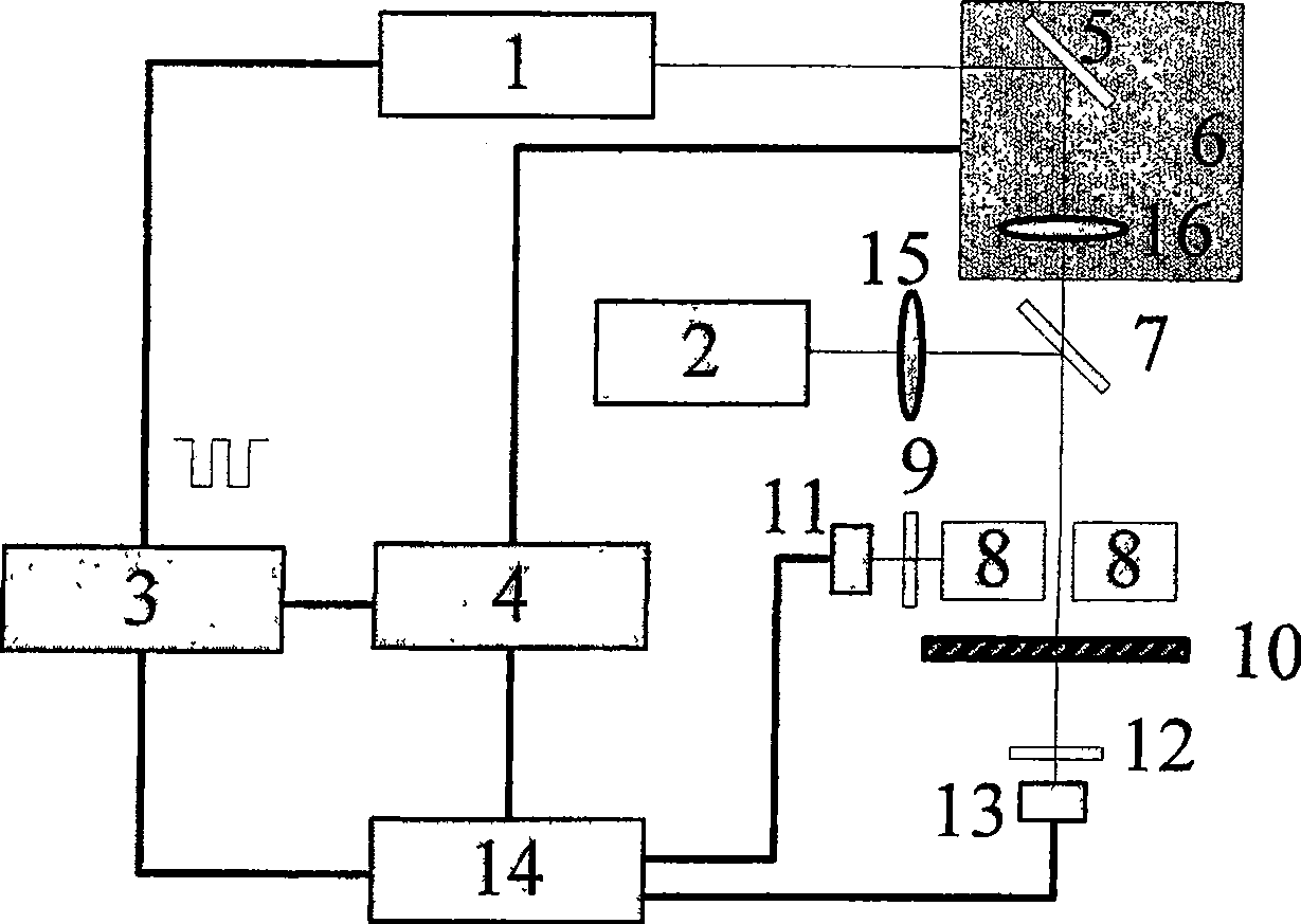
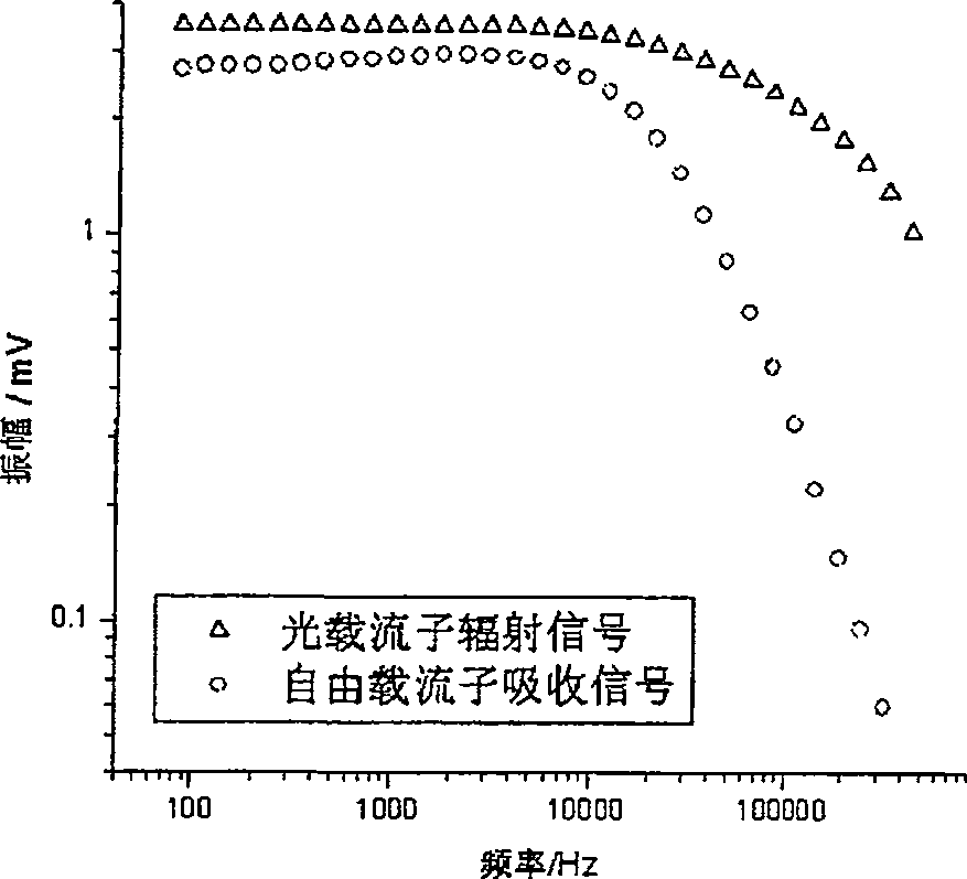
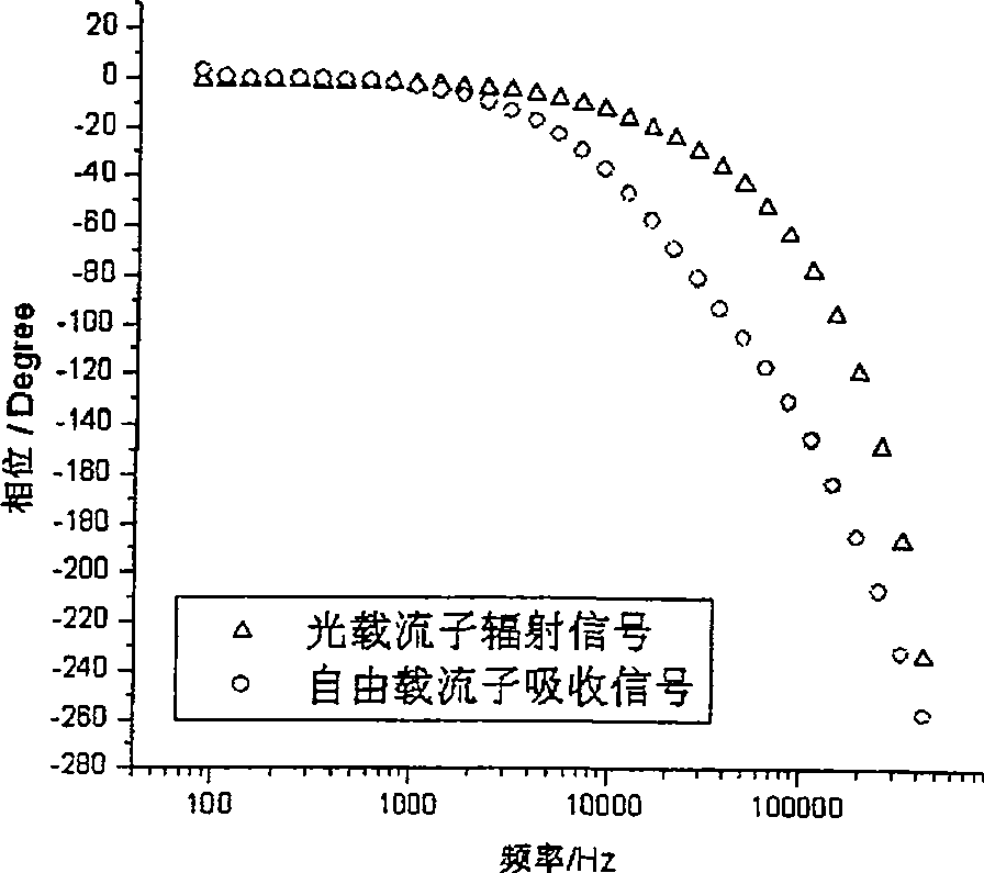
[0026] A specific embodiment of the present invention is given below: by this method, a silicon wafer sample is measured when the distance Δd=0 between two beams of light. The parameters of the silicon wafer sample used: P type, crystal orientation , resistivity 15-25Ω·cm, thickness 550μm, surface implanted with P ions.

[0027] Such as figure 1 As shown, the measuring device for realizing the present invention includes: an excitation laser light source 1, a detection laser light source 2, a signal generator 3, a computer 4, a mirror 5, a precision displacement stage 6, a beam splitter 7, a fluorescence collection system 8, an optical filter 9. Sample stage 10 , carrier radiation signal photodetector 11 , optical filter 12 , carrier absorption signal photodetector 13 , lock-in amplifier 14 , focusing lenses 15 and 16 . The signal generator 3 outputs a periodic square wave signal, and the signal frequency increases in a proportional sequence between 83Hz-436kHz, taking 32 poin...


PUM


Abstract

A method for measuring semiconductor doping concentration, characterized in that: photocarrier radiation measurement technology and free carrier absorption measurement technology are integrated in the same test system, and the composite radiation signal and absorption signal of free carriers are obtained at the same time ; By changing the modulation frequency of the excitation light, the carrier radiation signal and absorption signal in the frequency domain are obtained; by changing the distance between the excitation light and the probe light, the carrier radiation signal and absorption signal in the space domain are obtained; The carrier radiation signal and absorption signal data of the standard sample are compared to obtain the doping concentration of the tested sample. The invention is based on the optical carrier radiation measurement technology and the free carrier absorption technology, and greatly improves the measurement accuracy of the doping concentration because the information of the two independent signals in the frequency domain and the space domain is integrated.

Description

technical field [0001] The invention belongs to the technical field of non-destructive testing of semiconductor materials, in particular to a method for determining the doping concentration of semiconductors. Background technique [0002] From the perspective of semiconductor materials, the conductivity of intrinsic semiconductors is very poor. Only when a small amount of impurities are added to change the structure and resistivity, the semiconductor can become a useful functional material. Doping semiconductor materials is the basis of semiconductor devices, and the distribution of doping atoms directly affects the performance of semiconductor devices. Therefore, the precise monitoring and control of the impurity concentration and its uniformity in semiconductors is a very critical technical difficulty in semiconductor manufacturing technology. [0003] The common technologies currently used in the industry for on-line detection of impurity concentrations are the four-prob...

Claims


Application Information

Patent Timeline
Patent Type & Authority Patents(China)
IPC IPC(8): H01L21/66
Inventor 李斌成刘显明
Owner INST OF OPTICS & ELECTRONICS - CHINESE ACAD OF SCI
Why Eureka
Try Eureka