
Signal processing circuit of analog image for CMOS image sensor

A signal processing circuit and analog image technology, applied in the direction of image communication, television, electrical components, etc., can solve the problems of size reduction, circuit complexity, chip size increase, etc., and achieve the effect of reducing cost, reducing size, and simplifying circuit structure

Active Publication Date: 2008-12-17
BYD SEMICON CO LTD
View PDF3 Cites 2 Cited by
  • Summary
  • Abstract
  • Description
  • Claims
  • Application Information

AI Technical Summary

Problems solved by technology

[0007] When the CMOS image sensor in the prior art realizes differential work, and realizes color control, exposure control, black background control, dynamic noise elimination and fixed noise FPN, its processing circuit function is single and the circuit is complicated, so the size of the chip is increased. However, in today's fierce competition in the IC market, on the premise that the imaging effect is not affected, reducing the size and reducing the cost has become the focus of competition among CMOS image sensor design manufacturers

Method used


Image

  • Signal processing circuit of analog image for CMOS image sensor
  • Signal processing circuit of analog image for CMOS image sensor

Examples


Embodiment approach

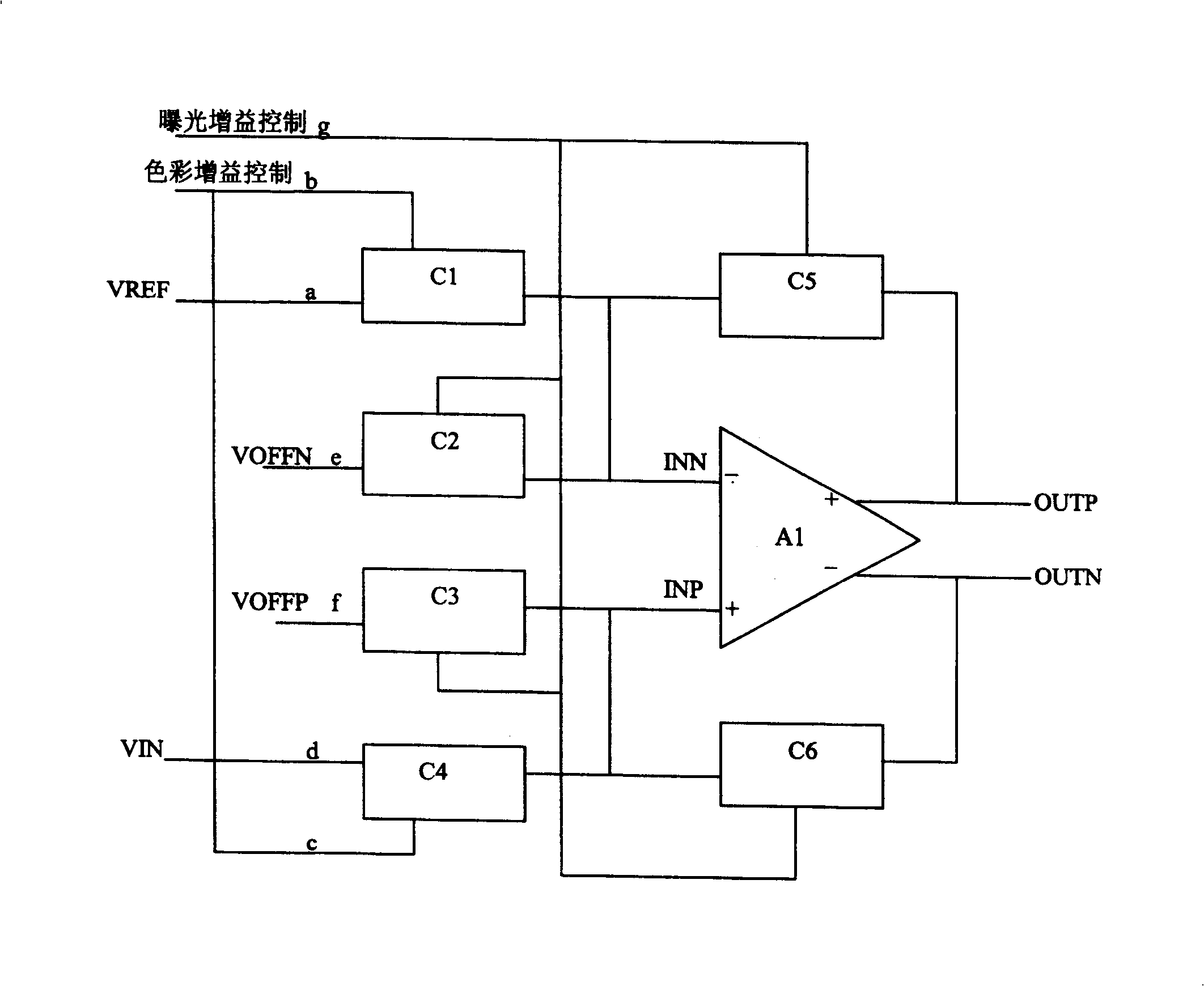
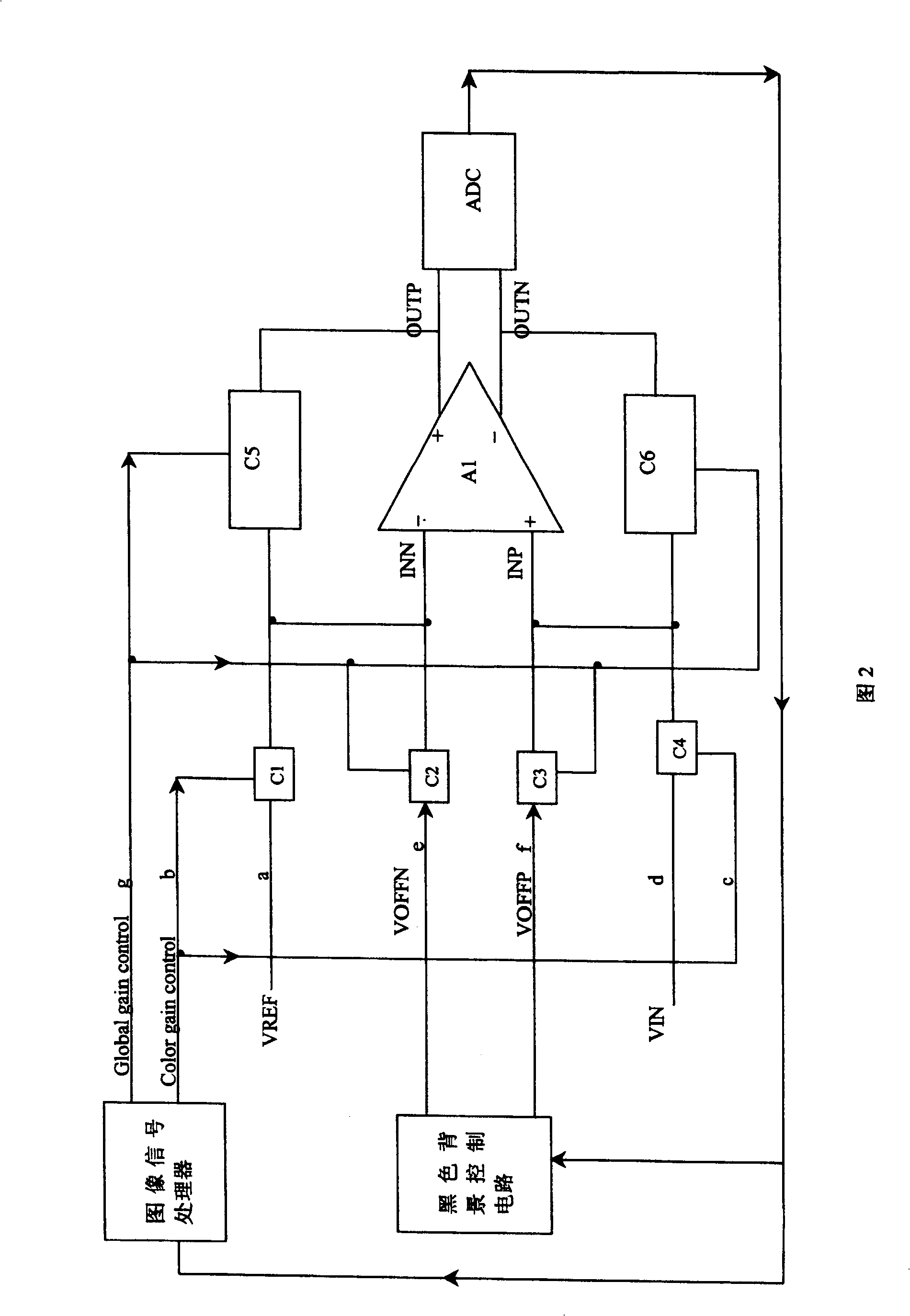
[0029] The present invention may also have other implementation manners, for example, the input stage capacitor may not include the second positive input stage switched capacitor array C3 and the second negative input stage switched capacitor array C2. This embodiment uses the same circuit to realize the color gain adjustment and the exposure gain adjustment, and at the same time eliminate the functions of dynamic noise and fixed noise FPN.

[0030] Figure 2 is a schematic diagram of the connection between the preferred embodiment of the present invention and other circuits. It can be seen from the figure that the output terminal of the differential operational amplifier A1 is connected to the analog-to-digital converter ADC, and the digital image processing ISP (image signal process) outputs colors according to the automatic adjustment function The gain signal b, exposure gain signal g, and color gain signal b are used to adjust the capacitance values ​​of the first positive inpu...


PUM


Abstract

The invention discloses an analog image signal processing circuit for a CMOS image sensor, which includes a differential operational amplifier, an input stage capacitor and an output stage capacitor. The input stage capacitor includes a first positive input stage switched capacitor array and a first negative input stage. Switched capacitor array; the input analog image signal of the first positive input switched capacitor array, the control terminal is connected to the color gain control signal terminal, and the output terminal is coupled to the input positive terminal of the differential operational amplifier; the input reference of the first negative input switched capacitor array Level signal, the control terminal is connected to the color gain control signal terminal, and the output terminal is coupled to the input negative terminal of the differential operational amplifier; the output stage capacitor is connected between the output terminal and the input terminal of the differential operational amplifier. The present invention uses one circuit to realize two or more control functions. On the premise of ensuring the imaging effect, the circuit structure is simplified, the size of the CMOS image sensor chip is reduced, the cost is reduced, and it is in line with the development trend of product miniaturization.

Description

【Technical Field】 [0001] The present invention relates to a CMOS (complementary metal oxide semiconductor) image sensor, and more particularly to a circuit for analog image signal processing in the CMOS image sensor. 【Background technique】 [0002] With the continuous improvement of CMOS process and solid-state image sensor technology, CMOS image sensor has developed rapidly. CMOS image sensor technology has replaced CCD sensor technology in the low-end image and video market. CMOS image sensor has more advantages than CCD image sensor. Low power consumption, wide dynamic range, high-speed video, high integration, low cost and other advantages, suitable for miniature digital cameras, portable video phones, computer cameras and other fields, CMOS image sensors can also be used for military reconnaissance, satellites, etc. [0003] In order to facilitate the back-end digital image processing, usually there is an A / D converter in the CMOS image sensor chip to convert the analog imag...

Claims


Application Information

Patent Timeline
Patent Type & Authority Patents(China)
IPC IPC(8): H04N5/14H04N5/335H04N25/00
Inventor 胡文阁
Owner BYD SEMICON CO LTD
Learn More