


Quick Research
Generate reliable direction feasibility study reports for your R&D in just a few steps.

Technical Q&A
Discover and master advanced knowledge NOW. Basics, ideas, possibilities, all at once.

Find Solutions
As an expert in R&D theories, this can generate solutions to your technical problems instantly.

Evaluate Feasibility
Analyze your overall solution with one click, know your potential R&D risks in advance.

Monitor Landscape
Get weekly tech updates, stay abreast of the latest tech innovations and key insights.
Heat sink of encapsulation through high frequency in use for semiconductor laser modulated by electrical absorption
An electro-absorption modulation and semiconductor technology, which is applied in the heat sink field of high-frequency packaging of electro-absorption modulation semiconductor lasers, can solve the problems affecting the high-frequency performance of the device packaging module and serious microwave loss, so as to improve the overall high-frequency dynamic performance, The effect of small reflection parameters and shortening the length of the connecting gold wire
- Summary
- Abstract
- Description
- Claims
- Application Information
AI Technical Summary
Problems solved by technology
Method used
Image

Examples
Embodiment Construction
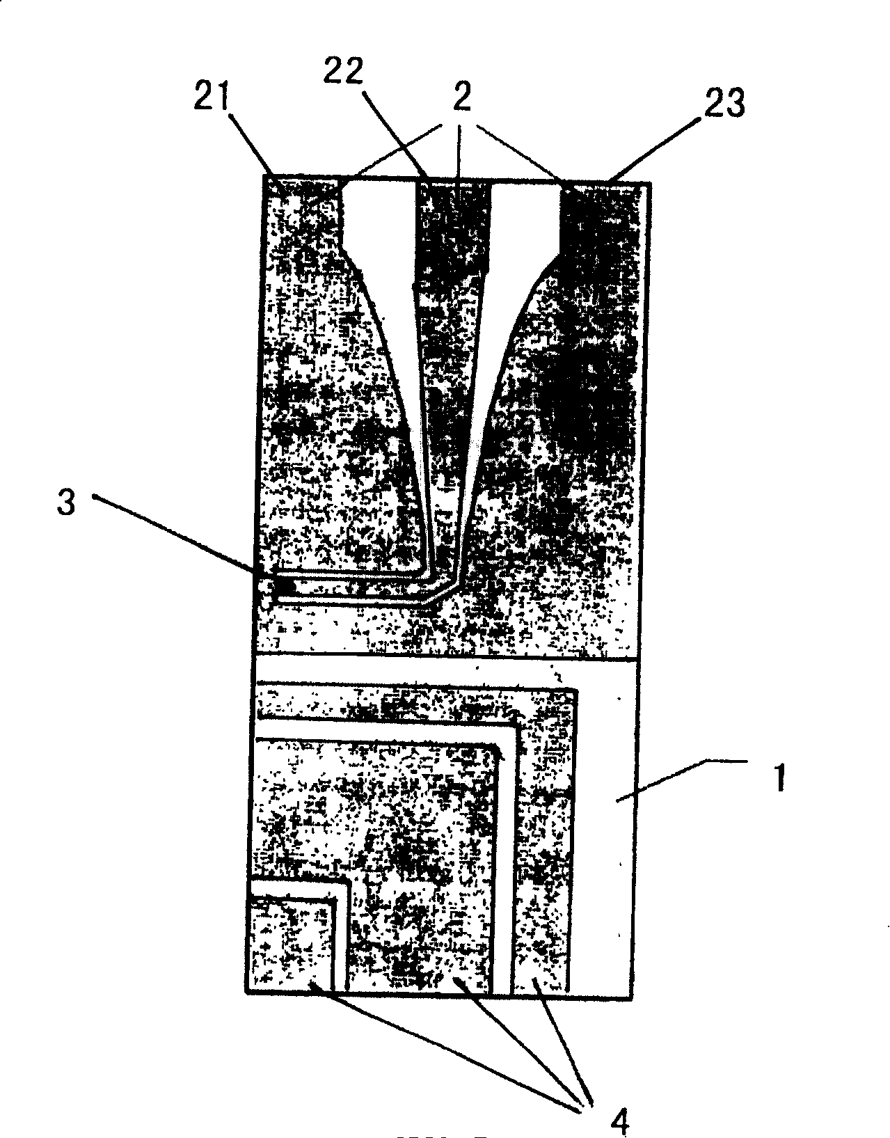
[0021] see figure 1 and figure 2 , which includes:
[0022] A dielectric heat sink substrate 1, what the dielectric heat sink substrate 1 adopts is aluminum nitride (AlN) or aluminum oxide (Al 2 o 3 ) or silicon carbide (SiC) or beryllium oxide (BeO) or beryllium nitride (BN) or diamond material, the substrate material requires good electrical properties (small dielectric constant, low dielectric loss, good thermal properties, High thermal conductivity) and a thermal expansion coefficient that matches the semiconductor material of the chip. At the same time, there are also requirements for the flatness and roughness of the substrate;
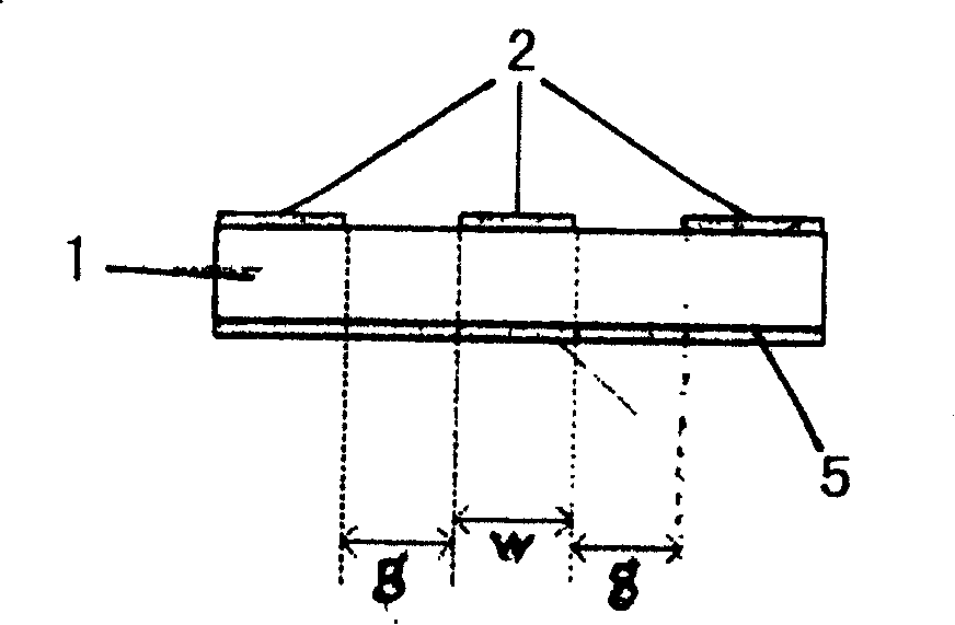
[0023] A microwave transmission line 2, the microwave transmission line 2 adopts a coplanar waveguide transmission line (the coplanar waveguide transmission line is also represented by a label 2), a coplanar waveguide (CPW) transmission line 2, the characteristic impedance of the coplanar waveguide (CPW) transmission line 2 is 50Ω , the met...
PUM
 Abstract
Description
Claims
Application Information
 - R&D Engineer
- R&D Manager
- IP Professional
- Industry Leading Data Capabilities
- Powerful AI technology
- Patent DNA Extraction
Browse by: Latest US Patents, China's latest patents, Technical Efficacy Thesaurus, Application Domain, Technology Topic, Popular Technical Reports.
© 2024 PatSnap. All rights reserved.Legal|Privacy policy|Modern Slavery Act Transparency Statement|Sitemap|About US| Contact US: help@patsnap.com