Method and system for observing all signals inside programmable digital IC chip

A technology of integrated circuits and chips, which is applied in the field of testing and verification of programmable digital integrated circuit chips, and can solve the problems of multiple on-chip resources, occupation, and inability to be used in ASICs.

Inactive Publication Date: 2007-11-21
长江微电子技术(大连)有限公司
View PDF4 Cites 0 Cited by
  • Summary
  • Abstract
  • Description
  • Claims
  • Application Information

AI Technical Summary

Problems solved by technology

In order to save the output of all memory, it takes a lot of on-chip resources
[0007] (2) Because it takes up a lot of on-chip resources, the functions that can be realized by the FPGA chip are very small, and the operating frequency is also very low.
[0008] (3) Since the on-chip memory cannot be made very large, the length of the saveable waveform is very short
[0009] (4) Only the output data of the on-chip memory can be seen, but the contents of all units of the on-chip memory cannot be seen
Benchtop logic analyzers with large memory depths are very expensive
[0011] (6) Only applicable to FPGA, not ASIC
When designing an ASIC, after the first release, there are often errors

Method used


Image

  • Method and system for observing all signals inside programmable digital IC chip
  • Method and system for observing all signals inside programmable digital IC chip
  • Method and system for observing all signals inside programmable digital IC chip

Examples


Embodiment Construction

[0054] The present invention will be further described below in conjunction with the drawings and embodiments.

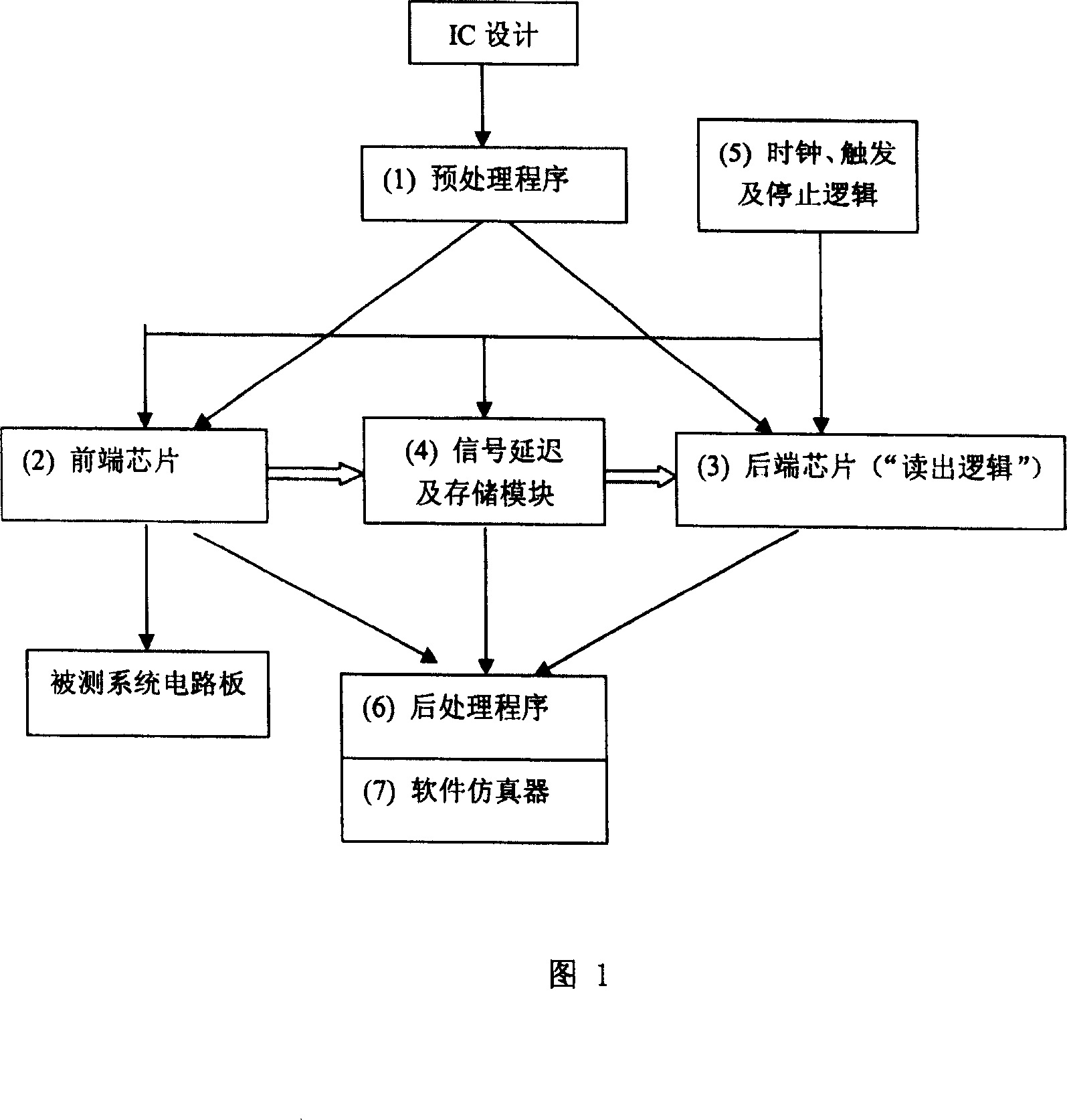
[0055] The whole test system is constituted as shown in Figure 4. The host can be a microcomputer or a workstation, and the pre-processing program, post-processing program, software simulator and system control program are all running on the host. The test system consisting of "back-end programmable digital integrated circuit chip", "signal, delay and storage module" and "clock, trigger and stop logic" is installed in a separate chassis, and its connection with the microcomputer is through PCI bus or USB bus. The "front-end programmable digital integrated circuit chip" is installed on the circuit board under test to realize real-time, online testing. A cable is used between the "front-end programmable digital integrated circuit chip" and the test system to send all the signals on the pins to the chassis of the test system.

[0056] In order to increase the transmission ...


PUM


Abstract

The present invention is method for real-time and on-line observing all the signal waveforms inside programmable digital IC chip, including various types of memory chip. The observing point may be any time after the measured system begins to operate, and the length of signal waveform to be collected is not limited by the internal resource of the programmable digital IC chip. The design of the digital IC is written into two identical programmable digital IC chips with similar operation process but a time difference of N clocks and capable of being stopped in any time instant. The states of chip registers and memories in the stop time may be read out and are combined with the signals collected from the chip pins to predict the state signals of the combination circuit inside the chip. Further processing of these data can obtain the waveforms of all the signals inside the chip.

Description

Technical field [0001] The invention relates to the testing and verification of programmable digital integrated circuit chips, in particular to a method and system capable of real-time and online observation of the waveforms of all signals in the programmable digital integrated circuit chip. The method and system can be used not only as a logic analyzer for testing circuit boards, but also as a hardware simulator for verifying IC design. Background technique [0002] With the development of semiconductor integrated circuit technology, the integration of chips is higher, and the functions of programmable digital integrated circuit chips are more complex. Programmable application specific integrated circuits (ASIC), field programmable gate arrays (FPGA) and programmable logic devices ( PLD) applications are very popular, and there has been a System On a Chip (SOC), that is, the entire system is integrated on a chip, not only has CPU, memory and I / O interfaces, but also complex algo...

Claims


Application Information

Patent Timeline
Patent Type & Authority Patents(China)
IPC IPC(8): H01L21/66G01R31/28G11C29/00
Inventor 刘建光
Owner 长江微电子技术(大连)有限公司
Why Eureka
Try Eureka