Semiconductor integrated circuit
a technology of integrated circuits and semiconductors, applied in the direction of semiconductor devices, basic electric elements, electrical appliances, etc., can solve the problems of inconvenient single-height configuration, inability to secure a space to connect the gates together with the upper layer wirings, and several gate lines that must be further shorted together, so as to reduce the number of internal wirings, eliminate waste of space, and increase the standard cell length of multi-height cells
- Summary
- Abstract
- Description
- Claims
- Application Information
AI Technical Summary
Benefits of technology
Problems solved by technology
Method used
Image
Examples
first embodiment
1. First Embodiment
1. Overall Layout
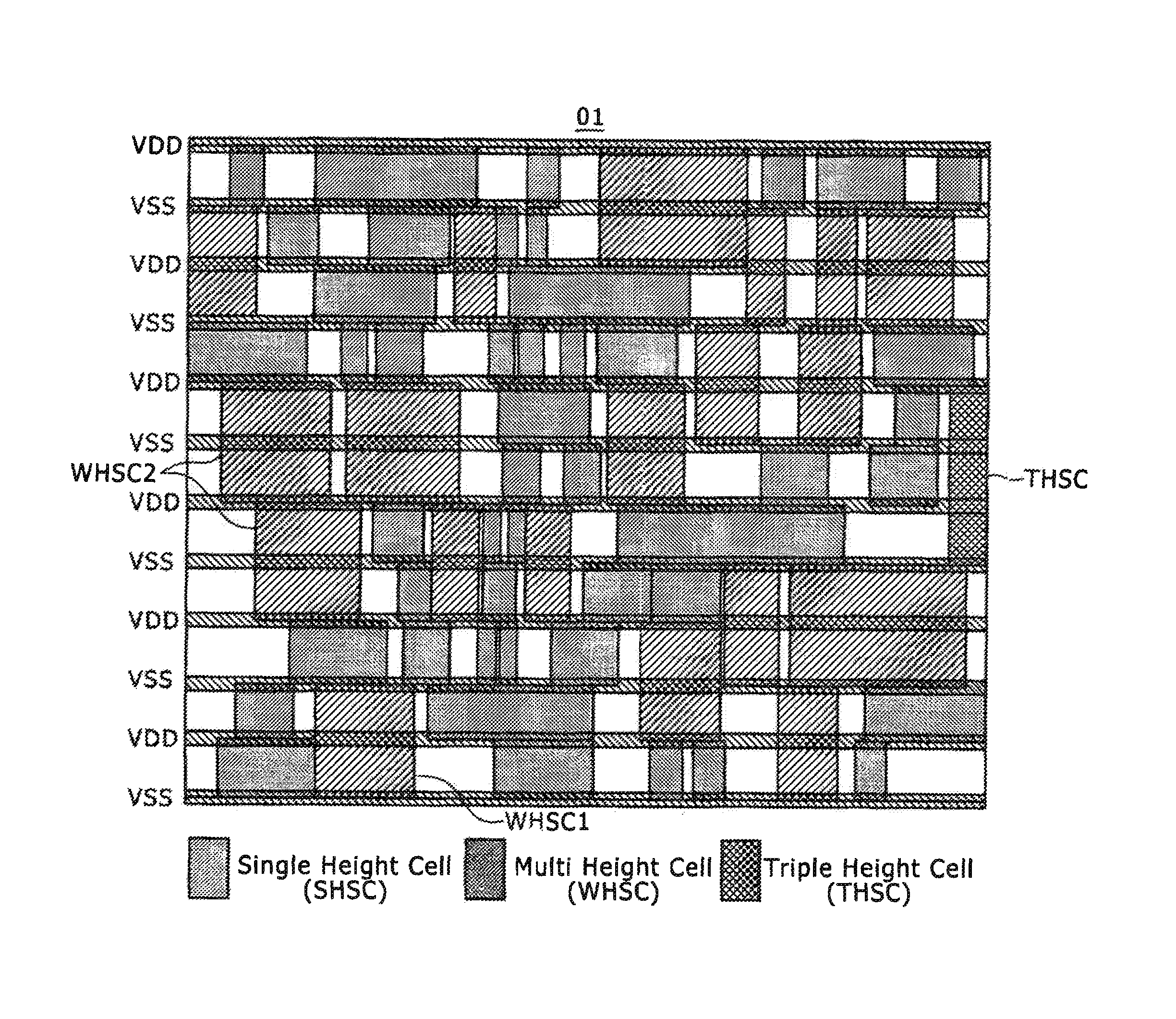
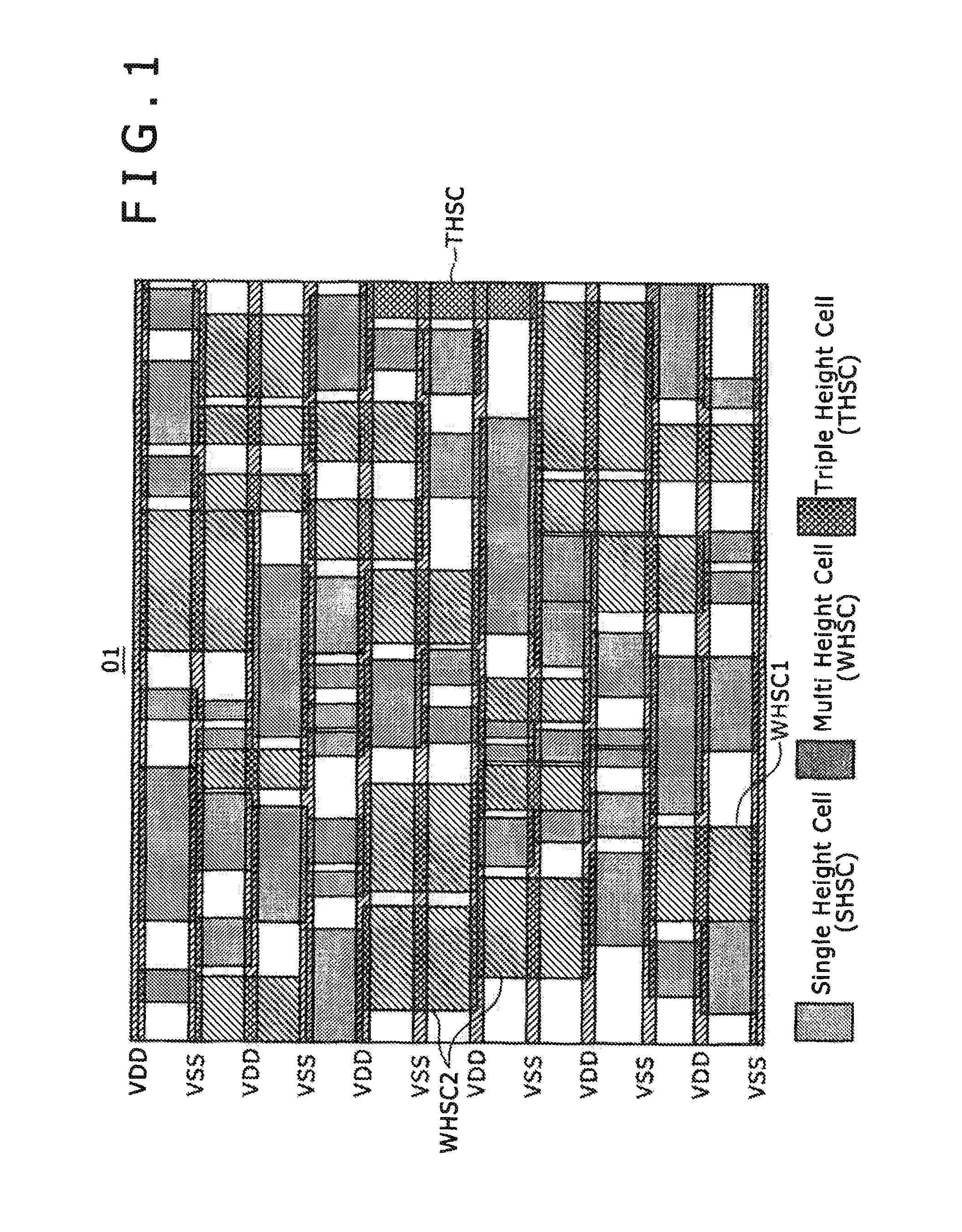
[0042]FIG. 1 is a diagram schematically illustrating a plan view of an integrated circuit according to embodiments with a focus on the cell layout.
[0043]In FIG. 1, each of rectangular areas is called a cell. The cells denoted by reference numeral SC are standard cells. The standard cell SC is a predesigned and standardized functional circuit cell registered in a library such as an inverter or a NAND gate. Although being a collection of data, the standard cell SC may refer to part of a device manufactured based on the data. Although a detailed description will be given later, standard cells registered in a library are combined and laid out in the design phase of a semiconductor integrated circuit. As a result of the layout, source voltage lines and reference voltage lines (e.g., GND lines) are roughly connected together on data. Connecting signal and other lines after the layout provides the desired circuit. The layout of cells and disposition of w...
first application example
[0065]FIG. 3 is an equivalent circuit diagram of a half adder cell as a circuit example of the standard cell SC to which the present invention is applied. The half adder shown in FIG. 3 is broadly divided into a carry-out section (CO section) and a single-bit addition section (Sum section). The half adder is a circuit designed to receive first and second input bits (A1 and A2) and output a half addition bit (S) and a carry-out bit (hereinafter the CO bit). The half addition bit represents the result of half addition in the first digit. The CO bit represents a carry.
[0066]It should be noted that the gates of the CMOS pairs that are supplied, for example, with the same input in FIG. 3 are indicated by bi-directional arrows.
[0067]The carry-out (CO) section includes a NAND circuit and an inverter. The NAND circuit includes two PMOS transistors P1 and P2 and two NMOS transistors N1 and N2. The inverter includes a PMOS transistor P3 and an NMOS transistor N3. The NAND circuit and inverter...
second application example
[0109]FIGS. 6A and 6B illustrate a circuit symbol and equivalent circuit diagram of a clock buffer cell.
[0110]A clock buffer cell is a cell including an even number of stages of cascaded inverters. This type of cell is designed so that the clock output from the cell has the same duty ratio to the extent possible. Therefore, a clock buffer is characterized in including larger-than-normal PMOS transistors or smaller-than-normal NMOS transistors.
[0111]A specific clock buffer circuit includes two cascaded inverters INV1 and INV2 shown in FIG. 6A. Each of the inverters INV1 and INV2 includes two inverters connected in parallel as shown in FIG. 6B. Thus, when each of the inverters INV1 and INV2 of the clock buffer at the first and second stages includes two inverters connected in parallel, the inverters offer sufficient driving capability. In addition, the present invention is more readily applicable to the clock buffer.
[0112]FIG. 7 illustrates an example in which the circuit shown in FIG...
PUM
 Abstract
Description
Claims
Application Information
 - R&D Engineer
- R&D Manager
- IP Professional
- Industry Leading Data Capabilities
- Powerful AI technology
- Patent DNA Extraction
Browse by: Latest US Patents, China's latest patents, Technical Efficacy Thesaurus, Application Domain, Technology Topic, Popular Technical Reports.
© 2024 PatSnap. All rights reserved.Legal|Privacy policy|Modern Slavery Act Transparency Statement|Sitemap|About US| Contact US: help@patsnap.com


