
System for measuring access time of memory

Active Publication Date: 2018-03-13
DONGBU HITEK CO LTD
View PDF5 Cites 2 Cited by
  • Summary
  • Abstract
  • Description
  • Claims
  • Application Information

AI Technical Summary

Benefits of technology

This patent is about a system that can accurately measure how long it takes to access a memory. This system can do it quickly and easily, and it can eliminate human error and errors that might occur during testing.

Problems solved by technology

As miniaturization of semiconductor manufacturing processes has increased, and SOC functionality has become more complex, the frequency of use and the capacity of embedded SRAMs have increased.
With process miniaturization, accurately measuring timing parameters such as access time on silicon has gradually become complicated and difficult, but the importance thereof has continually increased.

Method used


Image

  • System for measuring access time of memory
  • System for measuring access time of memory
  • System for measuring access time of memory

Examples


Embodiment Construction

[0043]Hereinafter, embodiments of the invention will be more clearly appreciated through the accompanying drawings and the following description thereof.

[0044]In the description of various embodiments, it will be understood that, when an element such as a layer (film), region, pattern or structure is referred to as being “on” or “under” another element, such as a substrate, layer (film), region, pad or pattern, it can be directly “on” or “under” the other element or be indirectly “on” or “under” the other element with intervening elements therebetween. It will also be understood that “on” and “under” the element is described relative to the drawings.

[0045]In addition, the relative terms “first” and “second”, “top / upper / above”, “bottom / lower / under” and the like in the description and claims may be used to distinguish between one substance or element and other substances or elements, and not necessarily for describing any necessary or required physical or logical relationship between ...


PUM


Abstract

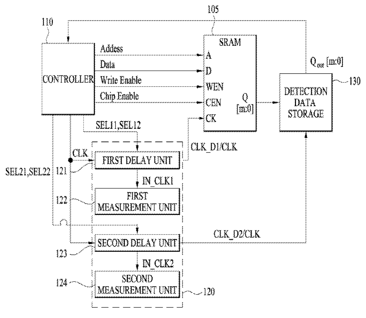
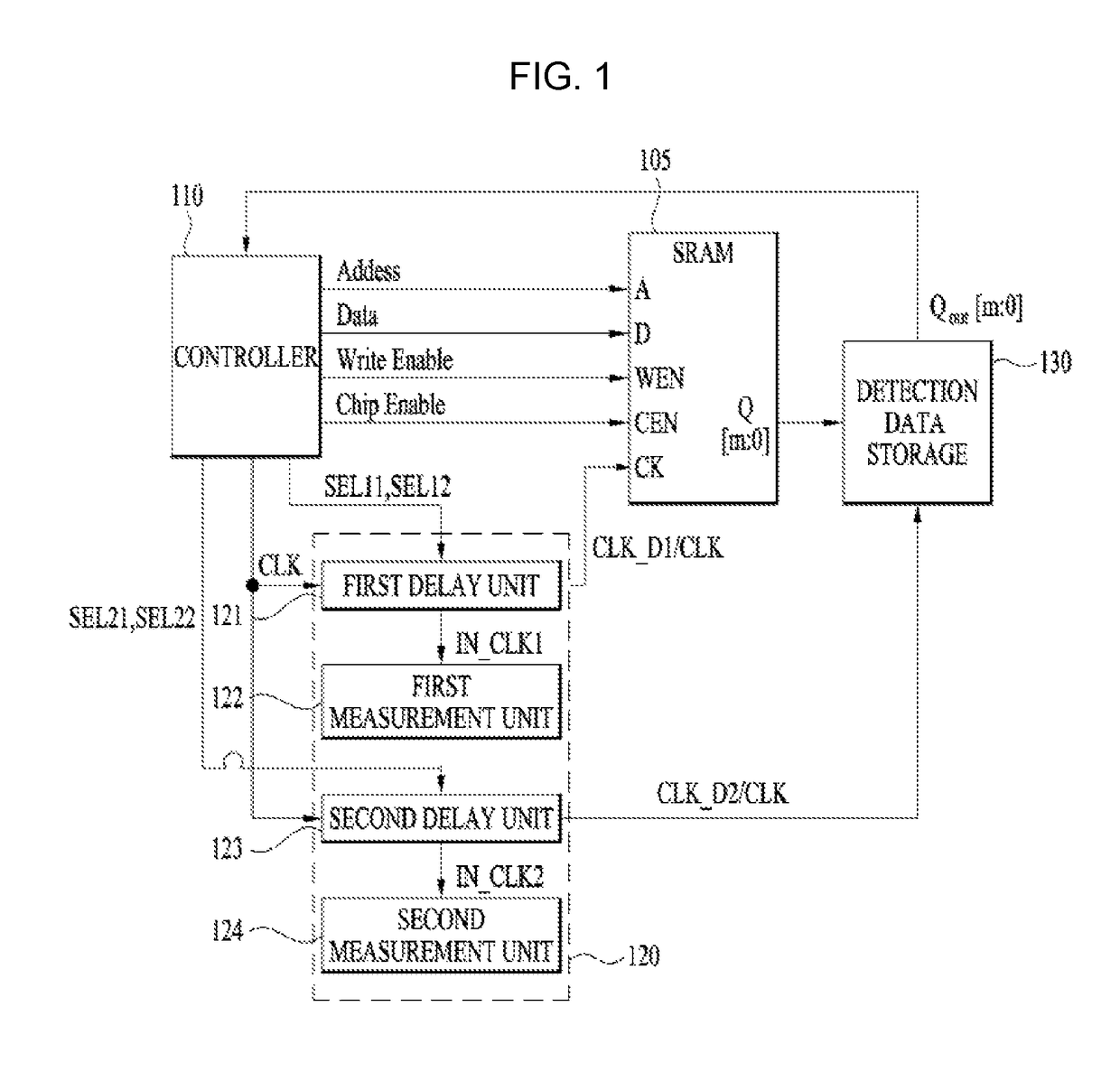
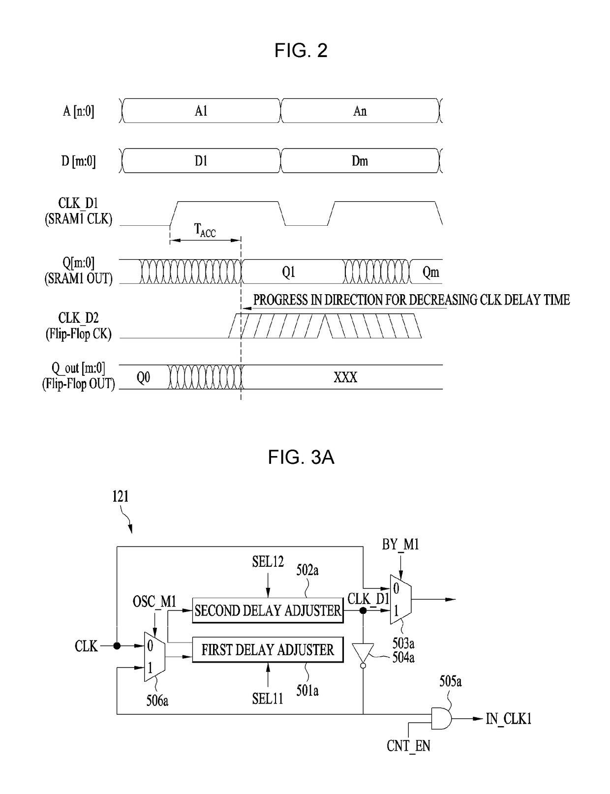
A system for measuring an access time of a memory includes a first delay unit configured to delay a clock signal by a first delay time and to output a first delayed clock signal, a second delay unit configured to delay the clock signal by a second delay time greater than the first delay time and to output a second delayed clock signal, a memory configured to store data, the data being read from the memory in response to the first delayed clock signal, a detection data storage configured to store the data read from the memory in response to the second delayed clock signal, and a controller configured to measure an access time of the memory based on a comparison of the data in the detection data storage and the data in the memory, the first delayed clock signal and the second delayed clock signal.

Description

[0001]This application claims the benefit of Korean Patent Application No. 10-2016-0156558, filed on Nov. 23, 2016, which is hereby incorporated by reference as if fully set forth herein.BACKGROUND OF THE INVENTIONField of the Invention[0002]Embodiments relate to a system for measuring an access time of an embedded memory.Discussion of the Related Art[0003]An embedded static random access memory (SRAM) is a device that can write or read data in or from a system on chip (SoC) logic circuit. As miniaturization of semiconductor manufacturing processes has increased, and SOC functionality has become more complex, the frequency of use and the capacity of embedded SRAMs have increased.[0004]The access time of the SRAM during operation is an important index, indicating the read speed of the SRAM. With process miniaturization, accurately measuring timing parameters such as access time on silicon has gradually become complicated and difficult, but the importance thereof has continually incre...

Claims


Application Information

Patent Timeline
IPC IPC(8): G11C11/41G11C11/413G11C29/50G11C8/18G11C29/04G11C7/22
CPCG11C11/413G11C29/50012G11C2029/0401G11C8/18G11C7/222G11C29/12015G06F11/3037
Inventor SHIN, WOO CHEOLBAEK, KYUNG ILJUNG, HYUN SUP
Owner DONGBU HITEK CO LTD
Learn More