Light emitting device, illuminating device and method of manufacturing light emitting device
a technology of light emitting devices and illumination devices, which is applied in the direction of semiconductor devices for light sources, semiconductor/solid-state device details, lighting and heating apparatus, etc., can solve the problems of difficult to improve heat radiation, reduce the optical reflectance of the substrate, and increase the heat radiation. , the effect of improving the reflectan
- Summary
- Abstract
- Description
- Claims
- Application Information
AI Technical Summary
Benefits of technology
Problems solved by technology
Method used
Image

Examples
first embodiment
[0112]The operation and effects of light emitting device 250 in accordance with the present embodiment are the same as those of the
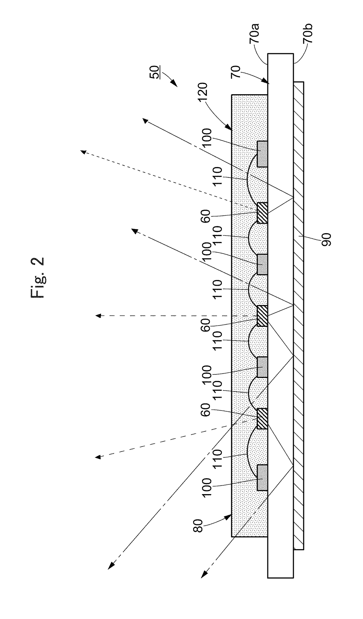
[0113]Referring to FIG. 10, a light emitting device 350 in accordance with the present embodiment includes a metal reflection film 390 in place of metal reflection film 90 (see FIG. 2) of light emitting device 50 (see FIG. 2) in accordance with the first embodiment. Metal reflection film 390 is formed of a reflection film of Al or its alloy. Specifically, though light emitting device 350 in accordance with the present embodiment is similar to light emitting device 50 in accordance with the first embodiment, it is different from light emitting device 50 including metal reflection film 90 formed of a reflection film of Ag or its alloy, in that metal reflection film 390 is formed of a reflection film of Al or its alloy.
[0114]The reflection film of Al refers to a metal film including a film of which composition contains Al as a main component and alloyed by ...
third embodiment
[0174]The method of manufacturing light emitting device 450 in accordance with the present embodiment is the same as that of the It is noted, however, that when the surface roughness of mounting surface 470a of ceramic substrate 470 is made larger than the surface roughness of non-mounting surface 470b, mounting surface 470a may be subjected to polishing process, as needed. The polishing process for mounting surface 470a may be the same as that for non-mounting surface 470b.
[0175]In the present embodiment, the surface roughness of mounting surface 470a of ceramic substrate 470 is made larger than the surface roughness of non-mounting surface 470b as described above, whereby the efficiency of extracting light reflected by metal reflection film 390 to the outside can be improved. Therefore, the reflectance of ceramic substrate 470 can be improved while heat radiation characteristic can be improved.
[0176]Further, when the surface roughness Ra of mounting surface 470a of ceramic subst...
fifth embodiment
[0218]In the fifth embodiment, a bulb-type light emitting lamp is described as an example of the illuminating device. The present invention, however, is not limited to such an embodiment. The illuminating device may be a light emitting lamp of a type other than bulb type. By way of example, the illuminating device may be a straight tube type light emitting lamp, or it may be a circular light emitting lamp. The light emitting device by itself may be used as a light source of other equipments.
[0219]In the fifth embodiment, an example in which a heat conductor of TIM is arranged between the ceramic substrate of light emitting device and the heat sink has been described. The present invention, however, is not limited to such an embodiment. The heat conductor may be other than TIM. The heat conductor other than TIM may include, for example, a heat conducting sheet, gel, and high heat-conducting adhesive. Alternatively, the ceramic substrate and the heat sink may be in direct contact with...
PUM
| Property | Measurement | Unit |
|---|---|---|
| Ra | aaaaa | aaaaa |
| thickness | aaaaa | aaaaa |
| thickness | aaaaa | aaaaa |
Abstract
Description
Claims
Application Information
 - R&D
- Intellectual Property
- Life Sciences
- Materials
- Tech Scout
- Unparalleled Data Quality
- Higher Quality Content
- 60% Fewer Hallucinations
Browse by: Latest US Patents, China's latest patents, Technical Efficacy Thesaurus, Application Domain, Technology Topic, Popular Technical Reports.
© 2025 PatSnap. All rights reserved.Legal|Privacy policy|Modern Slavery Act Transparency Statement|Sitemap|About US| Contact US: help@patsnap.com