Stable and reliable FinFET SRAM with improved beta ratio

a technology of finfet and beta ratio, which is applied in the direction of semiconductor devices, semiconductor/solid-state device details, electrical devices, etc., can solve the problems of unsatisfactory access and disturb, and achieve the effect of facilitating modulation stability of semiconductor memory devices

Inactive Publication Date: 2017-10-24
GLOBALFOUNDRIES US INC
View PDF9 Cites 5 Cited by
  • Summary
  • Abstract
  • Description
  • Claims
  • Application Information

AI Technical Summary

Benefits of technology

[0008]In yet another aspect, a method for forming a semiconductor memory device which includes, for instance, providing at least two mask layers over a pair of fin structures extended above a substrate, a first mask layer of the at least two mask layers being orthogonal to a second mask layer of the at least two mask layers, where the first mask layer of the at least two mask layers facilitates modulating stability of the semiconductor memory device, without affecting the second mask layer of the at least two mask layers.

Problems solved by technology

The unitary beta ratio, for instance, could lead to undesirable issues such as, access disturb.

Method used


Image

  • Stable and reliable FinFET SRAM with improved beta ratio
  • Stable and reliable FinFET SRAM with improved beta ratio
  • Stable and reliable FinFET SRAM with improved beta ratio

Examples


Embodiment Construction

[0020]Aspects of the present invention and certain features, advantages, and details thereof, are explained more fully below with reference to the non-limiting examples illustrated in the accompanying drawings. Descriptions of well-known materials, fabrication tools, processing techniques, etc., are omitted so as not to unnecessarily obscure the invention in details. It should be understood, however, that the detailed description and the specific examples, while indicating embodiments of the invention, are given by way of illustration only, and not by way of limitation. Various substitutions, modifications, additions and / or arrangements within the spirit and / or scope of the underlying inventive concepts will be apparent to those skilled in the art from this disclosure.

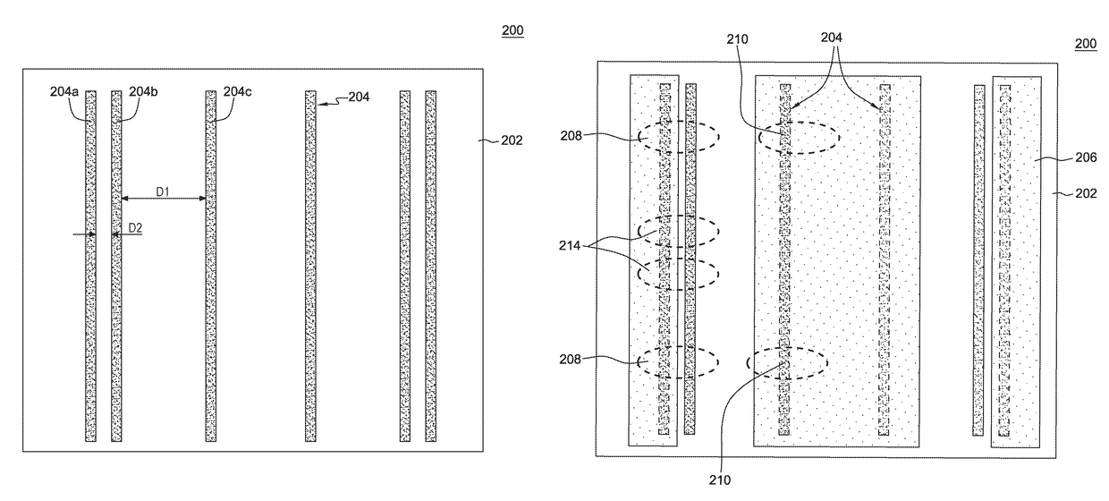
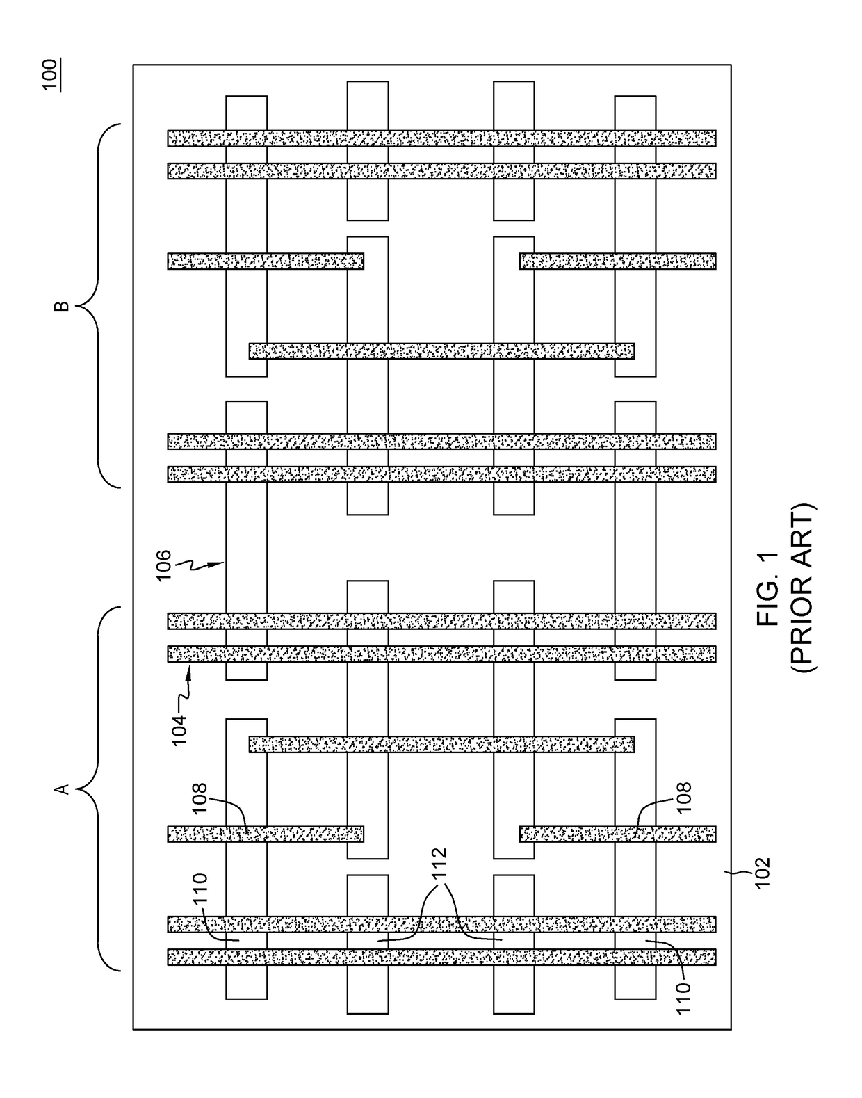
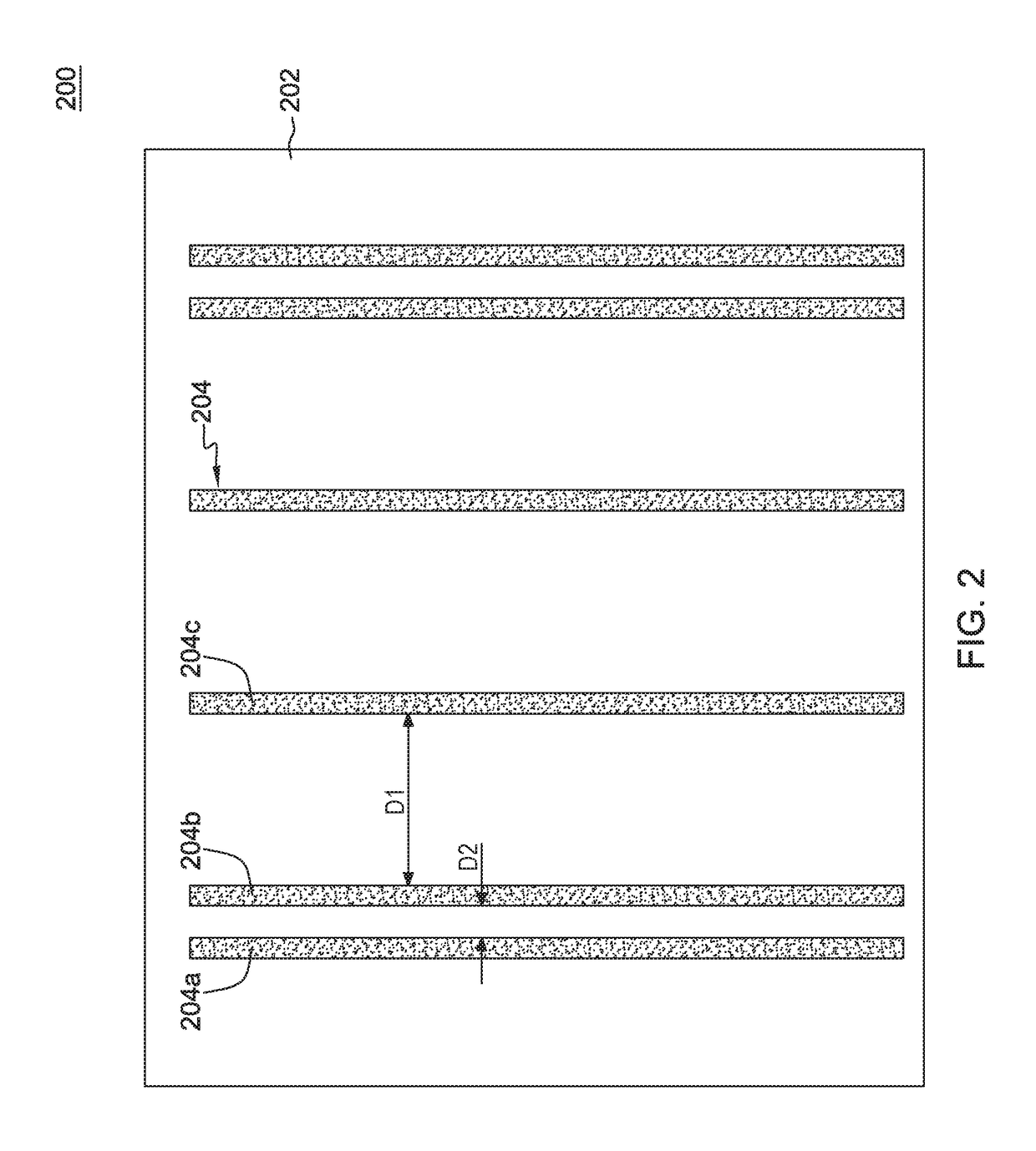
[0021]The present invention provides, inter alia, a fabrication method and a structure for a SRAM device with improved beta ratio. As described above, and in one aspect, during conventional FinFET fabrication processin...


PUM


Abstract

Fabrication method for a semiconductor memory device and structure are provided, which includes: providing at least two mask layers over a pair of fin structures extended above a substrate, wherein a first mask layer of the at least two mask layers is orthogonal to a second mask layer of the at least two mask layers; and patterning the pair of fin structures to define a pass-gate transistor, wherein the first mask layer facilitates removing of a portion of a first fin structure of the pair of fin structures to define a first pass-gate fin portion of the pass-gate transistor, and the second mask layer protects a second fin structure of the pair of fin structures to define a second pass-gate fin portion of the pass-gate transistor.

Description

FIELD OF THE INVENTION[0001]The present invention relates to a semiconductor memory device and to a method of fabricating a semiconductor memory device, and more particularly, to a static random access memory (SRAM) device with an improved beta ratio.BACKGROUND[0002]Conventional static random-access memory (SRAM) devices are generally used in applications requiring high speed, such as, memory in a data processing system, and typically consist of six transistors (6T): two P channel field effect transistors (PFETs) for a pull-up operation, two N channel field effect transistors (NFETs) for pull down, and two NFETs for input / output (i.e. passgate) access. As the size of technology nodes continues to decrease, fin field-effect transistors (FinFETs) are introduced to replace planar transistors, during the fabrication of SRAM devices. As one skilled in the art will understand, the stability of a 6T SRAM cell, in general, is defined by a beta ratio which, for instance, is the ratio of the ...

Claims


Application Information

Patent Timeline
Patent Type & Authority Patents(United States)
IPC IPC(8): H01L27/11H01L21/56H01L21/308H01L21/3065H01L23/31
CPCH01L27/1104H01L21/56H01L21/3085H01L21/3065H01L23/3171H01L27/0207H01L21/823431H10B10/12
Inventor WONG, ROBERT C.ZHUANG, LEIRAGHUNATHAN, ANANTHAN
Owner GLOBALFOUNDRIES US INC
Why Eureka
Try Eureka