Semiconductor device

a technology of semiconductors and semiconductor substrates, applied in semiconductor/solid-state device details, cooling/ventilation/heating modification, semiconductor devices, etc., can solve problems such as ceramic substrate breakage and ceramic substrate warpage, and achieve the effect of suppressing ceramic substrate warpag

Active Publication Date: 2017-08-01
MITSUBISHI ELECTRIC CORP
View PDF39 Cites 0 Cited by
  • Summary
  • Abstract
  • Description
  • Claims
  • Application Information

AI Technical Summary

Benefits of technology

[0008]The present invention has been made in light of the above-described problems. An object of the present invention is to provide a semiconductor device capable of suppressing warpage in a ceramic substrate.
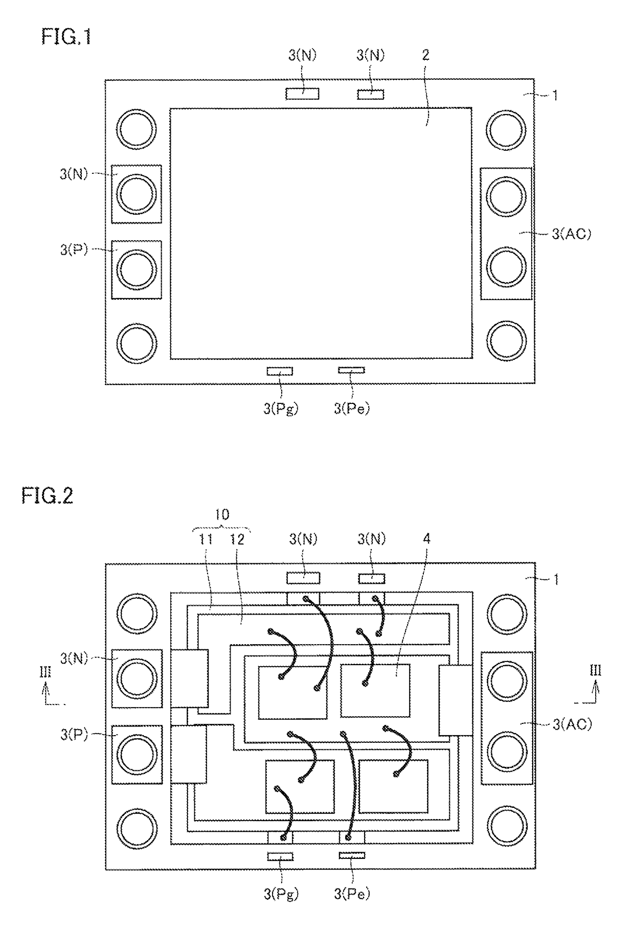
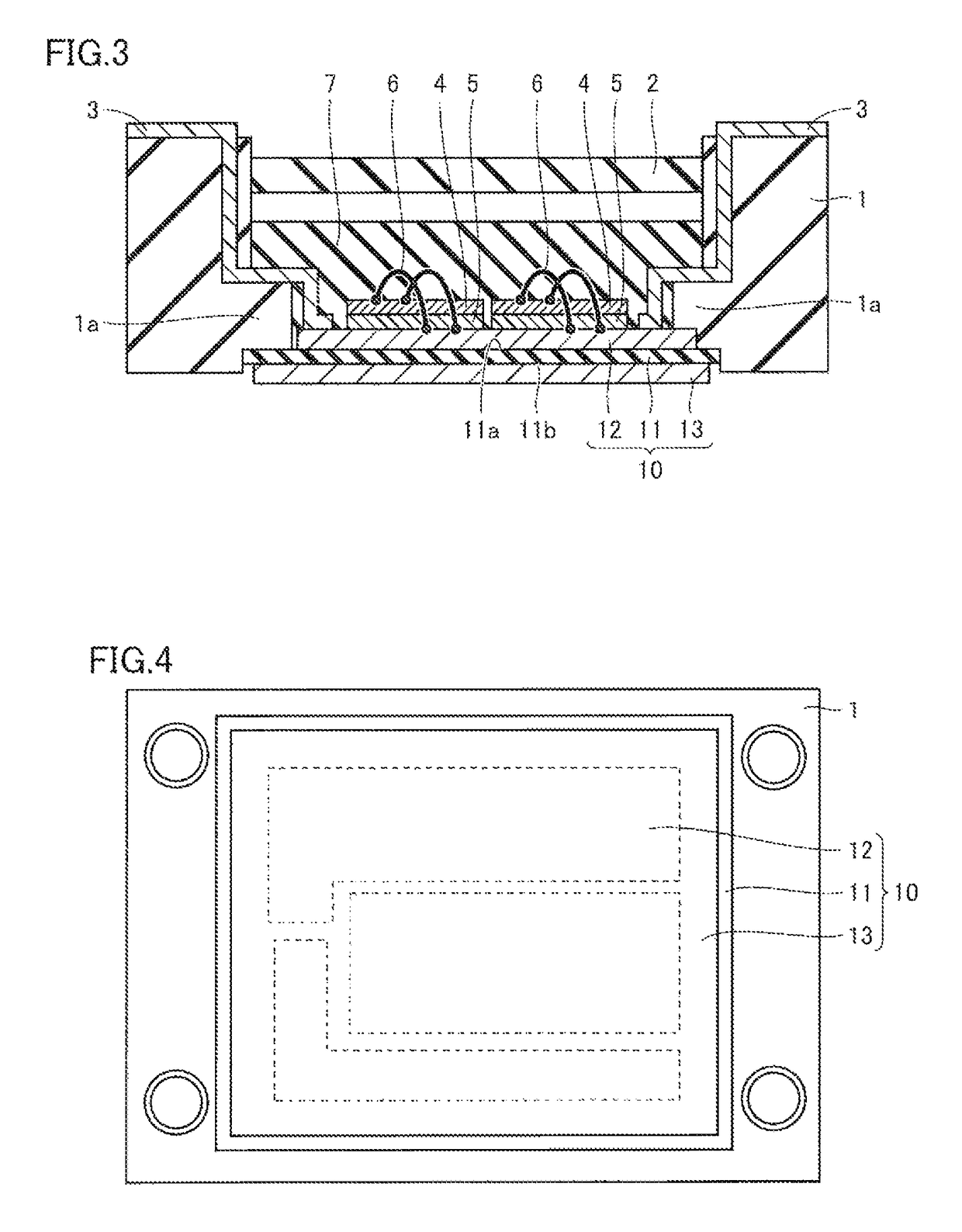
[0010]According to the semiconductor device of the present invention, the metal circuit board having a circuit pattern formed thereon is greater in thickness than the metal heat-dissipation plate. Also, the surface of the metal heat-dissipation plate on the side opposite to the ceramic substrate is larger in area than the surface of the metal circuit board on the side opposite to the ceramic substrate. Accordingly, the volume of the metal circuit board and the volume of the metal heat-dissipation plate can be balanced. Thereby, it becomes possible to suppress warpage of the ceramic substrate caused by thermal stress generated in the ceramic substrate. Therefore, breakage of the ceramic substrate can be suppressed.

Problems solved by technology

Accordingly, warpage occurs in the ceramic substrate.
Accordingly, large warpage occurs in the ceramic substrate, which may lead to breakage of the ceramic substrate.

Method used


Image

  • Semiconductor device
  • Semiconductor device
  • Semiconductor device

Examples


examples

[0077]Examples of the present invention will be hereinafter described.

[0078]First, the thermal resistances of the semiconductor device of the present invention example and the conventional semiconductor device were measured by simulation. Referring to FIG. 10, the thermal resistance of the semiconductor device will be described using the conventional semiconductor device as an example. The conventional semiconductor device includes a base plate 30. Each thermal resistance between corresponding points Tj, Tc, Tf, and Ta and the thermal resistance between point Tj and point Ta shown in FIG. 10 were measured. Point Tj is located on the upper surface of a semiconductor chip. Point Tc is located at the contact between base plate 30 and grease 21. Point Tf is located at the contact between grease 21 and heat sink 20. Point Ta is located on the lower surface of the heat sink. Furthermore, the semiconductor device of the present invention example does not include a base plate. In the presen...


PUM

PropertyMeasurementUnit
energy band gapaaaaaaaaaa

Abstract

A semiconductor device includes a semiconductor element and a ceramic circuit substrate on which the semiconductor element is mounted. The ceramic circuit substrate includes a ceramic substrate having one surface and the other surface facing each other, a metal circuit board joined to the one surface of the ceramic substrate and electrically connected to the semiconductor element, and a metal heat-dissipation plate joined to the other surface of the ceramic substrate. The metal circuit board is greater in thickness than the metal heat-dissipation plate. A surface of the metal heat-dissipation plate on a side opposite to the ceramic substrate is larger in area than a surface of the metal circuit board on a side opposite to the ceramic substrate. Thereby, a semiconductor device capable of suppressing warpage of the ceramic substrate can be achieved.

Description

BACKGROUND OF THE INVENTION[0001]Field of the Invention[0002]The present invention relates to a semiconductor device, and particularly to a semiconductor device including a ceramic circuit substrate.[0003]Description of the Background Art[0004]Conventionally, a ceramic circuit substrate has been used in a power semiconductor device such as a GTO (Gate Turn Off Thyristor) and an IGBT (Insulated Gate Bipolar Transistor). In this ceramic circuit substrate, a ceramic substrate has one surface to which a metal circuit board is joined and the other surface to which a metal heat-dissipation plate is joined. Then, a semiconductor element is mounted on the metal circuit board, and a heat sink is joined to the metal heat-dissipation plate.[0005]Since the metal circuit board is greater in coefficient of thermal expansion than the ceramic substrate, the metal circuit board expands more than the ceramic substrate due to the heat produced when using the semiconductor element. Accordingly, warpage...

Claims


Application Information

Patent Timeline
Patent Type & Authority Patents(United States)
IPC IPC(8): H05K7/20H01L23/498H01L23/057H01L23/24H01L23/373H01L23/36H01L23/473
CPCH01L23/24H01L23/057H01L23/36H01L23/3735H01L23/49811H01L2224/48091H01L2224/49113H01L2224/73265H01L2924/181H01L2924/19107H01L2924/00014H01L2924/00012H01L24/45H01L2224/45124H01L2224/29101H01L2224/32225H01L2224/48227H01L24/32H01L24/29H01L24/73H01L2224/4911H01L24/49H01L2924/13091H01L2924/13055H01L2924/014H01L2924/00H01L24/00
Inventor OTSUBO, YOSHITAKATAKAHASHI, TAKUYAMIYAZAWA, MASAOMIYAMASHITA, TETSUOHIEDA, TOMOHIROTABATA, MITUHARU
Owner MITSUBISHI ELECTRIC CORP
Why Eureka
Try Eureka