Semiconductor structure and manufacturing method thereof

a technology of semiconductor devices and manufacturing methods, applied in the direction of semiconductor devices, electrical devices, transistors, etc., can solve the problems of influencing the formation of epitaxial layers afterward, and achieve the effects of improving the performance of semiconductor devices, improving process convenience, and increasing quality of epitaxial layers

Active Publication Date: 2016-11-22
MARLIN SEMICON LTD
View PDF8 Cites 10 Cited by
  • Summary
  • Abstract
  • Description
  • Claims
  • Application Information

AI Technical Summary

Benefits of technology

[0008]The feature of the present invention is each fin structure is partially removed during the process for forming the fin structure, and the removed region is used for growing the epitaxial layer. In this way, the quality of the epitaxial layer can be increased, thereby improving the semiconductor device performance. Besides, the epitaxial layer of the present invention contacts more than one fin structure. In other words, the source / drain regions of a plurality of transistors can be formed simultaneously, and further improves the convenience of the process.

Problems solved by technology

Nevertheless, conventional FinFET fabrication of forming recesses after removing part of fin-shaped structures to accommodate the growth of epitaxial layer typically causes the fin-shaped structures to be lower than the surrounding shallow trench isolation (STI) as a result of over-etching, thereby influencing the formation of epitaxial layer afterwards.

Method used


Image

  • Semiconductor structure and manufacturing method thereof
  • Semiconductor structure and manufacturing method thereof
  • Semiconductor structure and manufacturing method thereof

Examples


Embodiment Construction

[0015]To provide a better understanding of the present invention to users skilled in the technology of the present invention, preferred embodiments are detailed as follows. The preferred embodiments of the present invention are illustrated in the accompanying drawings with numbered elements to clarify the contents and the effects to be achieved.

[0016]Please note that the figures are only for illustration and the figures may not be to scale. The scale may be further modified according to different design considerations. When referring to the words “up” or “down” that describe the relationship between components in the text, it is well known in the art and should be clearly understood that these words refer to relative positions that can be inverted to obtain a similar structure, and these structures should therefore not be precluded from the scope of the claims in the present invention.

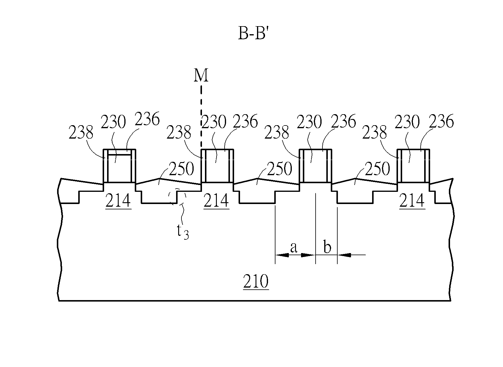
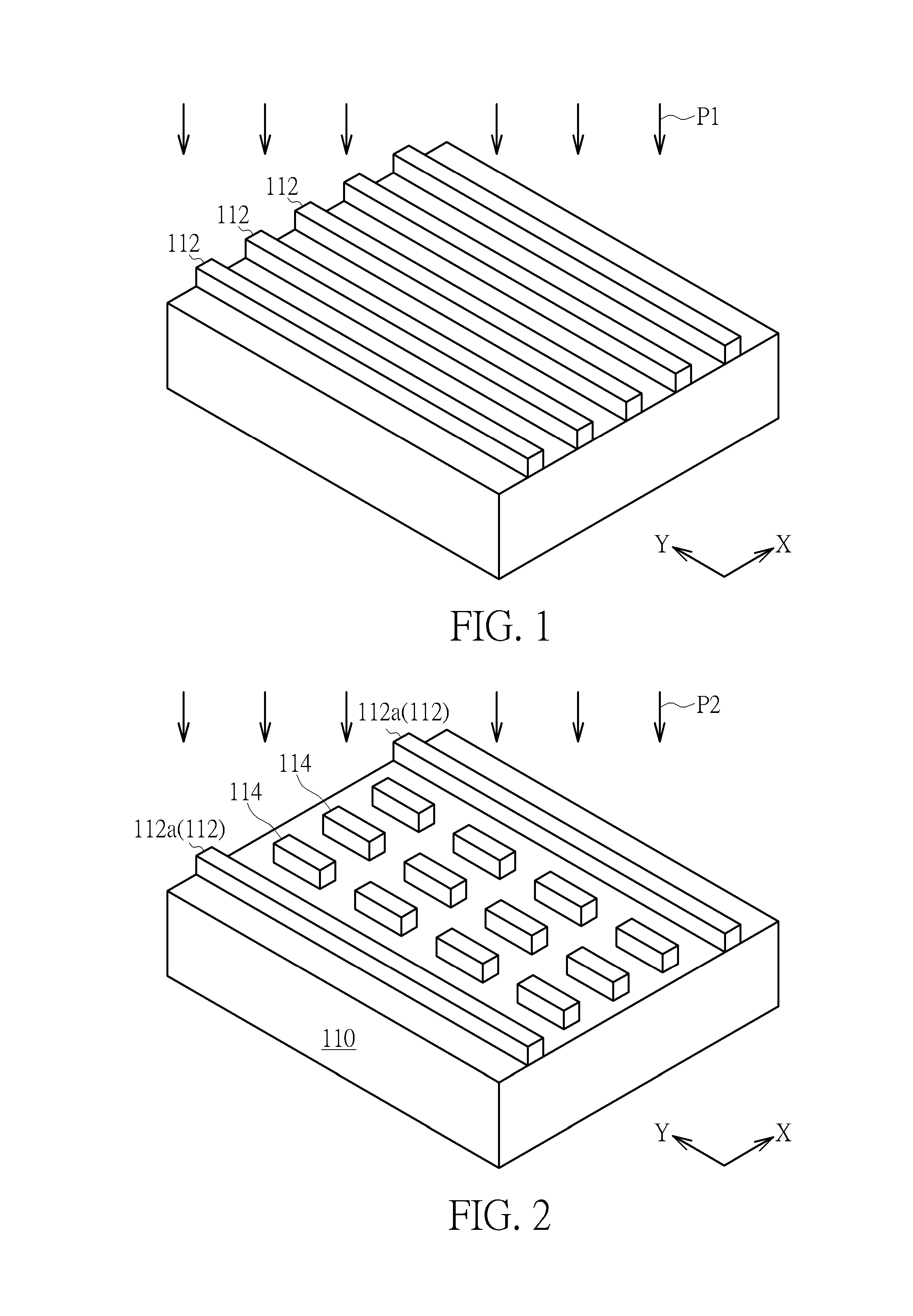
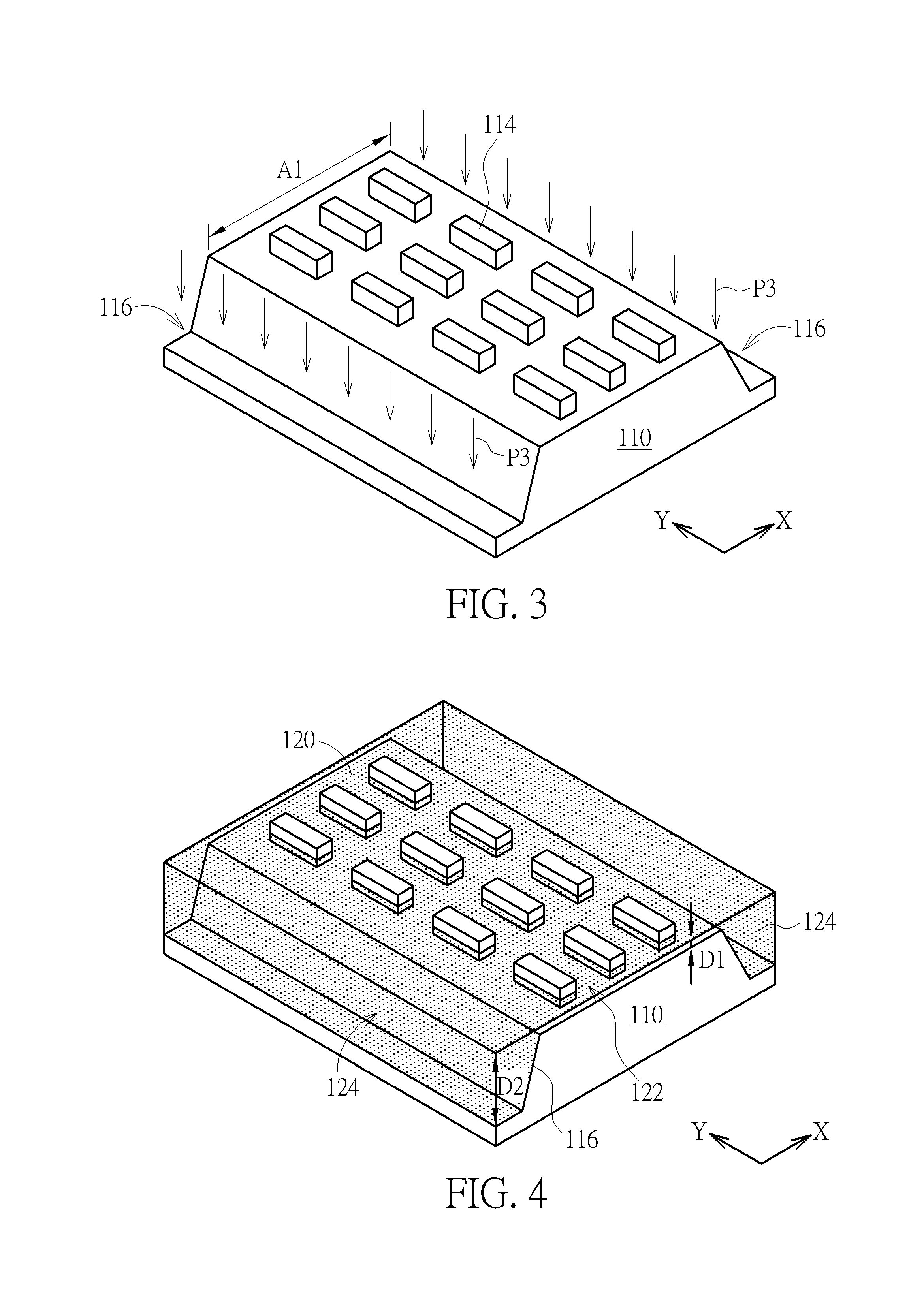
[0017]FIG. 1 to FIG. 8 are schematic diagrams showing a method for fabricating a semiconductor stru...


PUM


Abstract

The present invention provides a semiconductor structure, including a substrate having a first fin structure and a second fin structure disposed thereon, a first isolation region located between the first fin structure and the second fin structure, a second isolation region located opposite the first fin structure from the first isolation region, and at least an epitaxial layer disposed on the side of the first fin structure and the second fin structure. The epitaxial layer has a bottom surface, the bottom surface extending from the first fin structure to the second fin structure, and the bottom surface is lower than a bottom surface of the first isolation region and a top surface of the second isolation region.

Description

BACKGROUND OF THE INVENTION[0001]1. Field of the Invention[0002]The invention relates to a semiconductor structure and fabrication method thereof, and more particularly, to a semiconductor structure with better quality epitaxial layer.[0003]2. Description of the Prior Art[0004]With the trend in the industry being towards scaling down the size of the metal oxide semiconductor transistors (MOS), three-dimensional or non-planar transistor technology, such as fin field effect transistor technology (FinFET) has been developed to replace planar MOS transistors. Since the three-dimensional structure of a FinFET increases the overlapping area between the gate and the fin-shaped structure of the silicon substrate, the channel region can therefore be more effectively controlled. This way, the drain-induced barrier lowering (DIBL) effect and the short channel effect are reduced. The channel region is also longer for an equivalent gate length, thus the current between the source and the drain i...

Claims


Application Information

Patent Timeline
Patent Type & Authority Patents(United States)
IPC IPC(8): H01L27/088H01L21/762H01L21/306H01L29/78H01L21/28H01L21/8234H01L29/06H01L27/092
CPCH01L27/0886H01L29/0649H01L21/823431H01L21/823481H01L21/76224H01L21/30604H01L29/7842H01L29/785H01L27/092H01L27/088H01L29/1033H01L29/66795H01L29/165H01L21/845H01L27/1211H01L21/308H01L29/42372
Inventor FENG, LI-WEITSAI, SHIH-HUNGLIU, HON-HUEILIN, CHAO-HUNGHUANG, NAN-YUANJENQ, JYH-SHYANG
Owner MARLIN SEMICON LTD
Why Eureka
Try Eureka