Method of generating patterns on doubly-curved surfaces

a technology of doubly-curved surfaces and patterns, applied in the field of doubly-curved surfaces, can solve the problems of undesirable prior art of splicing flat sheets of etched conductors onto curved surfaces, difficulty in maintaining electrical conductivity across the surface, and difficulty in maintaining registration between layers, etc., to achieve rapid patterning of large areas, high speed, and high precision

Active Publication Date: 2016-08-30
II VI DELAWARE INC
View PDF15 Cites 6 Cited by
  • Summary
  • Abstract
  • Description
  • Claims
  • Application Information

AI Technical Summary

Benefits of technology

[0009]Disclosed herein is a three-dimensional direct write system capable of defining a plurality of elements across a large field of view using an ablative or actinic light source and multi-axis galvanometer scan system with appropriate optics for converging the light to a single focal point in three-dimensional space using software generated three-dimensional vector data and a system controlled by a computer controller. The direct write system scans a single focused beam of light across three-dimensional surfaces at a high rate of speed and with high precision, allowing for rapid patterning of large areas without translational movement of conventional machine tools. The direct write system may be coupled with additional multi-axis robots, for manipulation of the part and / or the direct write system, to coordinate patterning functions and robot motion to eliminate seams along the patterned surface. The system is also capable of patterning the interior of mostly enclosed surfaces, such as missile radomes, by reflection of the converging beam of light off of an appropriately positioned mirror to project the light perpendicular to the interior surface. The patterned surface may be large and continuous primarily in two-dimensions, rotationally symmetric about an axis, or of arbitrary shape and form. The direct write system is suitable for a wide variety of materials including photoimageable polymers, physical vapor deposited thin films, ceramic thick films (cermets), electrodeposited films, and ablative materials. The invention does not require a photomask (or optical mask) or original phototool to be fabricated, so adjustments to the part design can be made easily during manufacturing, without generating new costly tooling.

Problems solved by technology

The prior art of splicing flat sheets of etched conductors onto curved surfaces is undesirable as the pattern is not continuous, gaps are present at the joints of the spliced sheets, and electrical conductivity across the surface is not maintained.
With composite structures requiring multiple circuit layers, registration between layers may be difficult to maintain as the composite materials are generally opaque and layup is generally performed by hand.
Additionally, missile radome structures may be exposed to extreme heat (>600° C.) in service, damaging most polymeric substrates used in the splicing methodology, requiring an alternative approach.
In the prior art where an individual element is transferred from an optical mask onto a three-dimensional surface using laser ablation or exposure of photoresist and etching, i.e. photolithography, the speed at which elements can be generated on the part is limited by the speed of the multi-axis robot used to orient the patterning tool.
This type of system is capable of producing seam free patterns in a step and repeat fashion, but the individual elements are subject to distortion by projection errors when the image is formed on the three-dimensional surface.
Additionally, this technique is only amenable to repetitive patterns, and not for circuits requiring continuous, variable, or tailored patterns over large areas.
This technique is insufficient for patterning on the inside of long, small diameter, missile radome structures as the robotic positioning system and image projection system is unable to orient normal to the interior surface due to space constraints, with focal distances being relatively short for high resolution features.

Method used


Image

  • Method of generating patterns on doubly-curved surfaces
  • Method of generating patterns on doubly-curved surfaces
  • Method of generating patterns on doubly-curved surfaces

Examples


Embodiment Construction

[0039]The present invention will be described with reference to the accompanying figures where like reference numbers correspond to like elements.

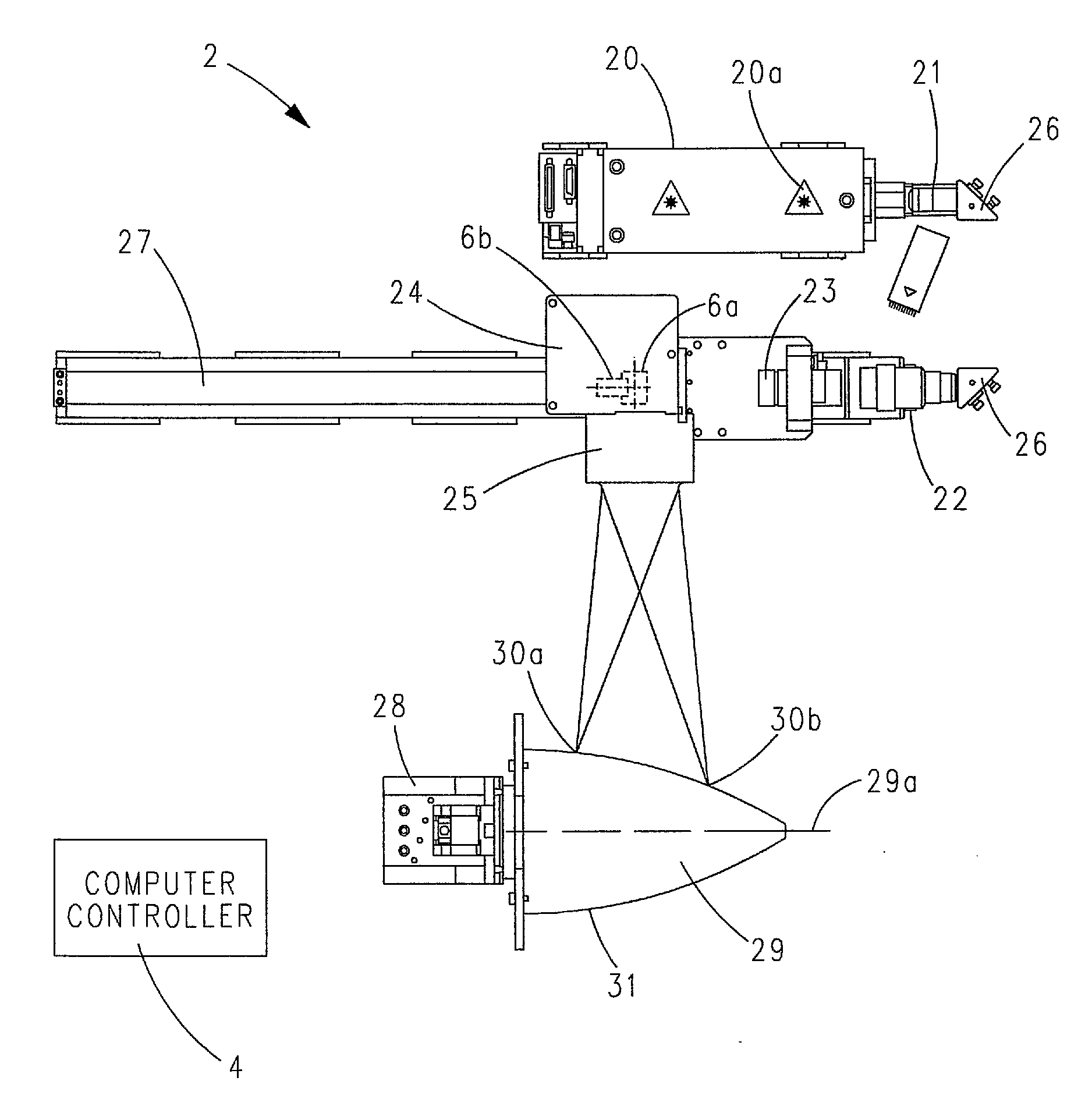
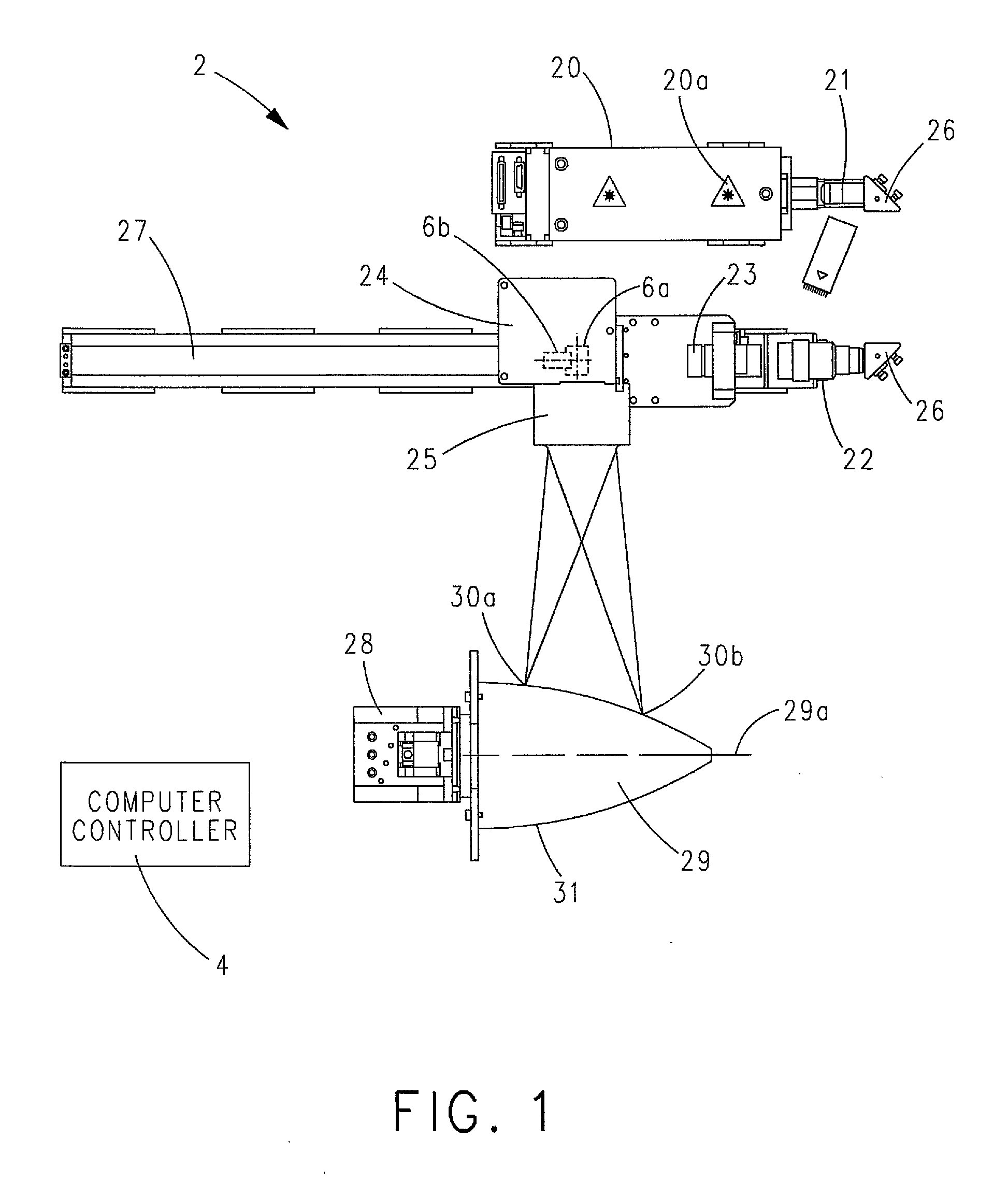
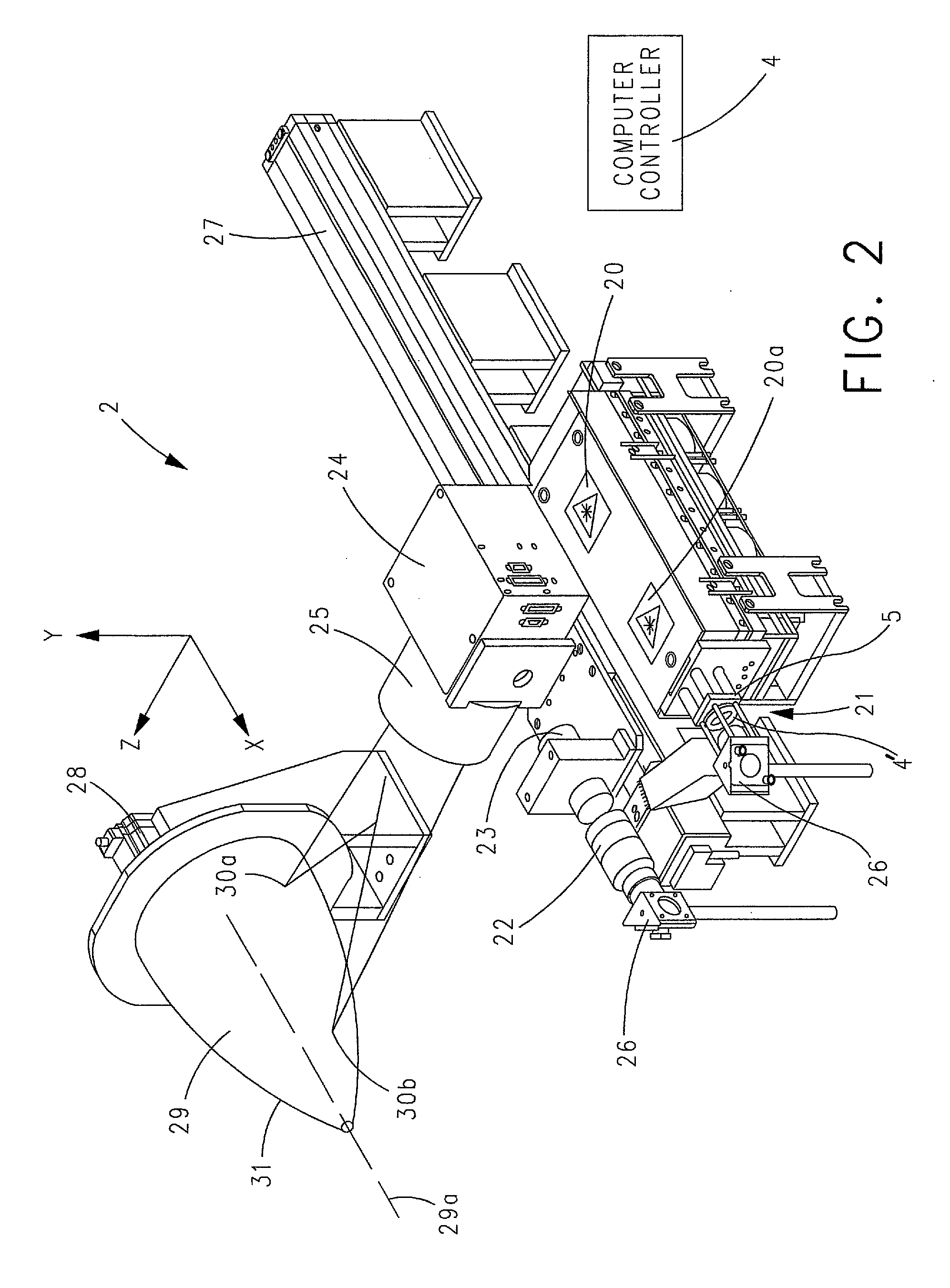
[0040]FIGS. 1-2 depict a multi-axis direct write system or robot 2 capable of patterning a rotationally symmetric, ogive (doubly-curved) surface 29 of a substrate 31, e.g., a dielectric radome. As used herein, “doubly-curved” means a surface which from a point thereon has a first radius of curvature in one direction (e.g., an X direction) and a second radius of curvature in a second, orthogonal direction (e.g., a Y direction).

[0041]A flow chart of the light propagation through an optical system of system 2 (and system 2′ shown in FIGS. 3A-4B) is shown in FIG. 5. In an exemplary case, the dielectric being patterned is a high temperature ceramic composite with low dielectric constant and loss tangent.

[0042]System 2 includes a light source 20 which may be an incoherent broadband light source, such as an ultraviolet mercury arc lamp; a monochr...


PUM

PropertyMeasurementUnit
output wavelengthsaaaaaaaaaa

Abstract

Disclosed is a system and method for patterning internal and / or external doubly-curved surfaces by use of a light source, three-dimensional scanning optics, computer controller, and a multi-axis robot. The system is capable of digitally receiving shape, location, and pattern data of a three-dimensional doubly-curved surface and applying said pattern over large areas with high precision in a seamless fashion.

Description

CROSS REFERENCE TO RELATED APPLICATION[0001]This application claims priority to U.S. Provisional Application No. 61 / 786,873, filed Mar. 15, 2013, which is incorporated herein by reference.BACKGROUND OF THE INVENTION[0002]1. Field of the Invention[0003]The present invention relates to electric or electronic circuits which are generated on a curved surface, especially a doubly-curved surface. The invention is especially useful for generating circuits requiring high precision, robust materials (high temperature or harsh environments), or multilayered designs where the circuits are stacked or embedded in additional dielectric or conductive layers. The invention is capable of generating conductive and dielectric patterns on otherwise undevelopable (doubly curved) three-dimensional surfaces.[0004]2. Description of Related Art[0005]In the aerospace and defense industries conformal electrical circuits are desirable for a variety of electrical means with regards to electromagnetic energy and...

Claims


Application Information

Patent Timeline
Patent Type & Authority Patents(United States)
IPC IPC(8): B23K26/046B29C59/16B23K26/08B23K26/00G03F7/20B23K26/36B29C35/08G03F7/24
CPCB29C59/165B23K26/362B23K26/0823B23K26/0084G03F7/70383G03F7/704B23K26/0066G03F7/24B29K2995/0005B29K2995/0006B29C2035/0827B29C2035/0833B29C2791/009B29C2035/0838B23K26/361B23K26/352B23K26/355
Inventor CASALE, DAVID M.ROLLINS, DEREK S.
Owner II VI DELAWARE INC
Why Eureka
Try Eureka