
Copper wiring forming method, film forming system, and storage medium

a technology of copper wiring and film forming, applied in the direction of vacuum evaporation coating, basic electric elements, coatings, etc., can solve the problem of difficult filling of cu into the recess, and achieve the effect of reducing the resistance and suppressing the increase of via resistan

Active Publication Date: 2016-08-23
TOKYO ELECTRON LTD
View PDF16 Cites 1 Cited by
  • Summary
  • Abstract
  • Description
  • Claims
  • Application Information

AI Technical Summary

Benefits of technology

The present invention provides a method for forming a copper wiring structure in contact with tungsten wiring by filling copper into a recess in a substrate. The method includes removing tungsten oxide from the surface of the tungsten wiring, forming a nitriding preventing film to prevent nitriding of the tungsten surface, applying a barrier film to prevent copper diffusion, and forming a liner film and copper film on top of the barrier film. The invention thus prevents an increase in via resistance and reduces overall resistance in the device.

Problems solved by technology

However, with the scaling dimension of the semiconductor device in recent years, it becomes difficult to fill Cu into the recess such as the fine trench or hole without causing voids by the conventional filling technology using plating after the barrier film and the Cu seed film are formed by PVD.

Method used


Image

  • Copper wiring forming method, film forming system, and storage medium
  • Copper wiring forming method, film forming system, and storage medium
  • Copper wiring forming method, film forming system, and storage medium

Examples


Embodiment Construction

[0025]Hereinafter, an embodiment of the present invention will be described referring to the drawings.

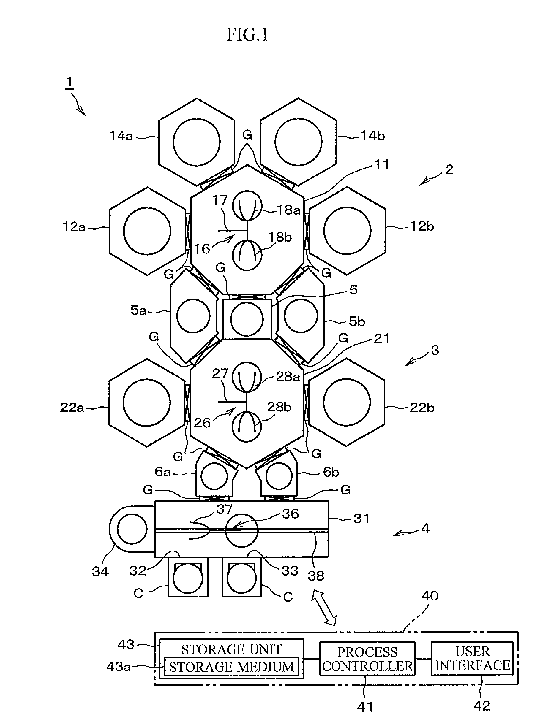
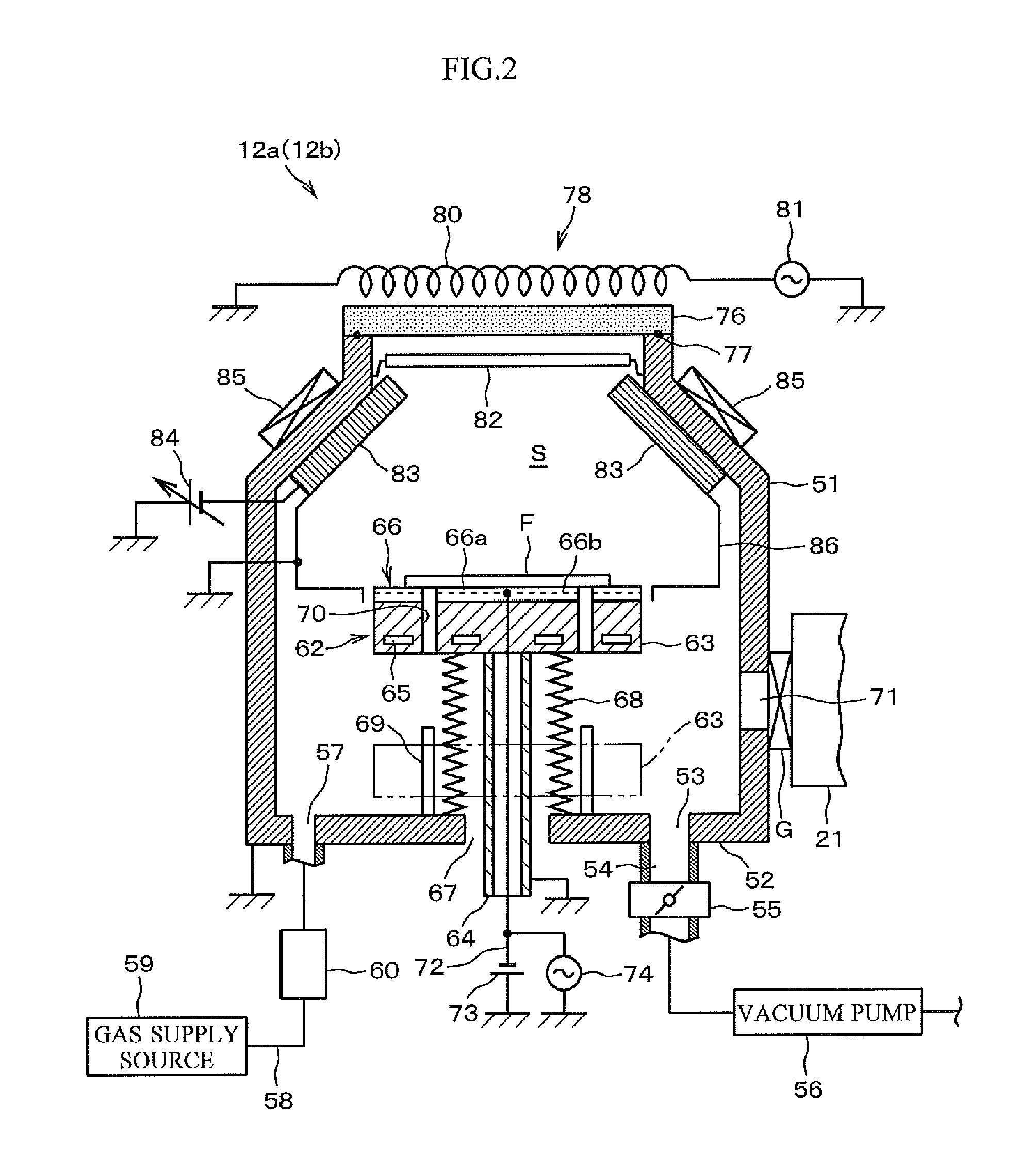
[0026]First of all, a film forming system used in the embodiment of the present invention will be described. FIG. 1 is a plan view illustrating an example of a multi-chamber film forming system for implementing formation of Cu wiring according to the embodiment of the present invention.

[0027]A film forming system 1 has: a first processing unit 2 that forms a nitriding preventing film, a barrier film, and a liner film; a second processing unit 3 that forms a Cu film; and a transfer-in / out unit 4, and is for forming Cu wiring on a semiconductor wafer (hereinafter, simply mentioned as a wafer) F.

[0028]The first processing unit 2 has a first vacuum transfer chamber 11 having a planar shape forming a heptagon, and two nitriding preventing film and barrier film forming apparatuses 12a, 12b and two liner film forming apparatuses 14a, 14b, which are connected to wall portions corresponding ...


PUM

PropertyMeasurementUnit
thicknessaaaaaaaaaa
temperatureaaaaaaaaaa
frequencyaaaaaaaaaa

Abstract

A Cu wiring forming method of forming Cu wiring that is to be arranged in contact with tungsten wiring, by filling Cu into a recess formed in a substrate, includes: removing a tungsten oxide formed on a surface of the tungsten wiring; forming a nitriding preventing film at least on the surface of the tungsten wiring in the recess; forming a barrier film that prevents diffusion of Cu, on a surface in the recess from above the nitriding preventing film; forming a liner film on the barrier film; and filling a Cu film on the liner film.

Description

BACKGROUND OF THE INVENTION[0001]1. Field of the Invention[0002]The present invention relates to a Cu wiring forming method of forming Cu wiring that is to be arranged in contact with tungsten wiring, by filling Cu in a recess such as a trench or hole formed in a substrate, a film forming system and a storage medium storing a program for controlling it.[0003]2. Description of the Related Art[0004]In manufacture of a semiconductor device, various processing such as film forming processing and etching processing on a semiconductor wafer are repeatedly performed to manufacture a desired device, and speed-up of the semiconductor device, shrinking of a wiring dimension, and denser integration are increasingly demanded. Since there is a need to reduce signal delay in order to increase the operating speed of the device, and also from the viewpoint of energy saving of the device, Cu wiring having an interlayer dielectric film lower in resistance and dielectric constant than aluminum (Al) an...

Claims


Application Information

Patent Timeline
Patent Type & Authority Patents(United States)
IPC IPC(8): H01L21/768H01L23/528H01L23/532H01L21/285C23C16/52C23C14/24C23C14/54C23C14/34
CPCH01L21/76879H01L21/76843H01L21/2855H01L21/28568H01L21/28556H01L23/53238H01L23/53266H01L23/53295C23C14/34C23C14/24C23C16/52C23C14/54H01L23/528C23C14/046C23C14/165H01L2924/0002H01L2924/00H01L21/76846
Inventor ISHIZAKA, TADAHIROSAKUMA, TAKASHIYOKOYAMA, OSAMUYU, KAI-HUNG
Owner TOKYO ELECTRON LTD
Learn More