Ionically permeable structures for energy storage devices
a technology of energy storage devices and ion permeable structures, which is applied in the direction of secondary cell servicing/maintenance, cell components, sustainable manufacturing/processing, etc., can solve the problems of crack formation, pulverisation of anodes, disintegration and exfoliation of existing electronic current collectors, etc., to reduce the weight and volume of inactive components and improve the efficiency of device packing
- Summary
- Abstract
- Description
- Claims
- Application Information
AI Technical Summary
Benefits of technology
Problems solved by technology
Method used
Image
Examples
example 1
Formation of an IPC Layer on a Monolithic Anode
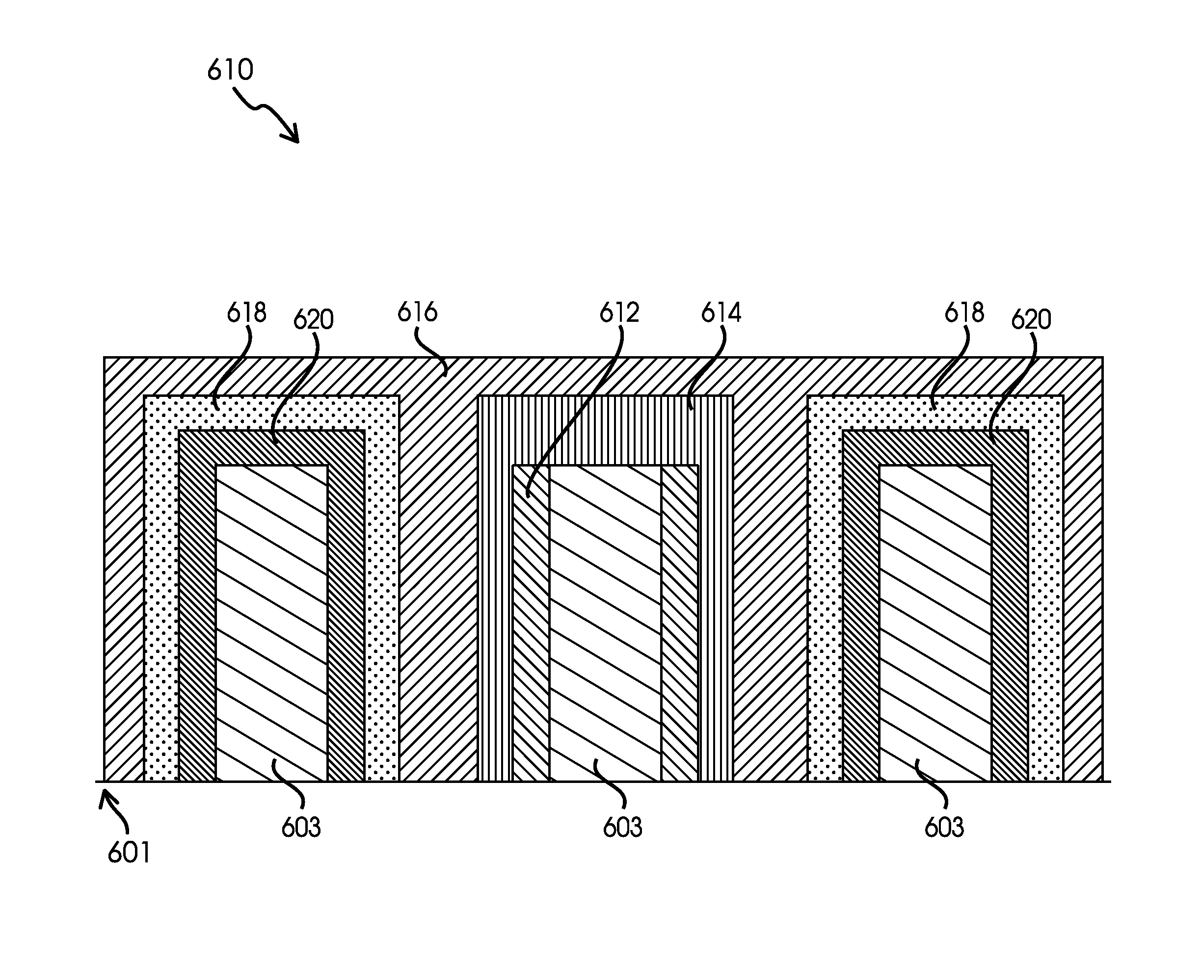
[0073]A Silicon substrate 500 μm thick is used as the starting material. The silicon substrate is cleaned and polished in 20% KOH solution at 65 C. for 3 minutes to clean the silicon surface. This sample is immersed in 500 milliliters of solution containing 0.1 M NiSO4.6H2O and 5M NH4F. The pH of the solution was maintained at 8.5 and the operating temperature was 85 C. The deposition time of the sample was 3 minutes. The sample was subsequently rinsed in DI water for 5 minutes and dried at 80 C. in air. Subsequently, the sample was annealed to a temperature of 550° C. for 20 minutes (including heating and cooling time) to form the silicide containing IPC layer.
example 1a
Formation of an IPC Layer on a Monolithic Anode
[0074]A Silicon substrate 500 μm thick is used as the starting material. The silicon substrate is cleaned and polished in 20% KOH solution at 65 C. for 3 minutes to clean the silicon surface. This sample is immersed in 500 milliliters of solution containing 0.1 M NiSO4.6H2O and 5M NH4F. The pH of the solution was maintained at 8.5 and the operating temperature was 85° C. The deposition time of the sample was 3 minutes. The sample was subsequently rinsed in DI water for 5 minutes and dried at 80° C. in air. Subsequently, the sample was annealed to a temperature of 550° C. for 20 minutes (including heating and cooling time) to form the silicide containing IPC layer. The excess Ni that did not form the silicide was selectively etched using a solution of 10% H2O2 and 10% H2SO4 for 10 minutes at 75° C.
example 1b
Formation of an IPC Layer on a Monolithic Anode
[0075]A Silicon substrate 500 μm thick is used as the starting material. The silicon substrate is cleaned and polished in 20% KOH solution at 65° C. for 3 minutes to clean the silicon surface. This sample is immersed in 500 milliliters of solution containing 0.1 M NiSO4.6H2O and 5M NH4F. The pH of the solution was maintained at 8.5 and the operating temperature was 85° C. The deposition time of the sample was 3 minutes. The sample was subsequently rinsed in DI water for 5 minutes and dried at 80° C. in air. Subsequently, the sample was annealed to a temperature of 300° C. for 5 minutes (including heating and cooling time) to improve the adhesion of deposited Ni to silicon. Since the deposit was based on a displacement nickel deposition, the Ni layer was porous and was able to allow the Lithium transport when assembled as an anode in a lithium battery.
PUM
| Property | Measurement | Unit |
|---|---|---|
| thickness | aaaaa | aaaaa |
| thickness | aaaaa | aaaaa |
| thickness | aaaaa | aaaaa |
Abstract
Description
Claims
Application Information
 - R&D
- Intellectual Property
- Life Sciences
- Materials
- Tech Scout
- Unparalleled Data Quality
- Higher Quality Content
- 60% Fewer Hallucinations
Browse by: Latest US Patents, China's latest patents, Technical Efficacy Thesaurus, Application Domain, Technology Topic, Popular Technical Reports.
© 2025 PatSnap. All rights reserved.Legal|Privacy policy|Modern Slavery Act Transparency Statement|Sitemap|About US| Contact US: help@patsnap.com


